Probe card for electronics devices

a technology for electronics devices and probes, applied in the direction of electronic circuit testing, measurement devices, instruments, etc., can solve the problems of affecting compromising the proper contact of the probe, and reducing the performance of the probe,

Active Publication Date: 2020-09-22
TECHNOPROBE
View PDF15 Cites 1 Cited by
  • Summary
  • Abstract
  • Description
  • Claims
  • Application Information

AI Technical Summary

Benefits of technology

[0031]It is an object of the present disclosure to provide a probe card for electronic devices integrated on wafers, having structural and functional characteristics so as to allow an adequate number of cleaning operation of the contact probes comprised into the corresponding testing head without functional loss, overcoming the limitations and the drawbacks that still afflict the testing heads realized according to the prior art, in particular by guaranteeing a constant exerted force and the essential scrub mechanisms for a proper contact between probes and contact pads throughout the entire working life of the probe card, even in case of subsequent cleaning operations.
[0058]joining again the testing head and the space transformer, so as to adjust the first length of the first terminal portion of the contact probes by changing the second length of the second terminal portion of the contact probes and restoring a proper working of the testing head and therefore of the probe card including it.

Problems solved by technology

The contact ends of the contact probes, in particular the contact tips with the pads of the devices to be tested, are subjected to accumulation of material, generally indicated as dirt, during their use, which decreases their performance and may compromise the proper contact of the probes with the device to be tested, when the scrub of these tips is not able to provide electrical contact with the pads anyway.
Obviously, such cleaning operations involve the consumption of a portion of the terminal portion of the probes, in particular of the contact tip, and are therefore limited in number precisely by the length of that tip, which becomes shorter at each cleaning.
Although advantageous in various respects, such testing head has a drawback due to the fact that the variation in the length of the terminal portions by means of the removal of the spacer or of a layer thereof inevitably also modifies the air or bending zones of the contact probes, thereby modifying the contact dynamics and introducing problems in terms of the force exerted by the probes on the contact pads and also of the scrub allowed on them, in addition to modifying the deformation suffered by the probes in such free zone, with the risk of permanent deformations or entrapments of such probes in the respective guide holes.

Method used


Image

  • Probe card for electronics devices
  • Probe card for electronics devices
  • Probe card for electronics devices

Examples


Embodiment Construction

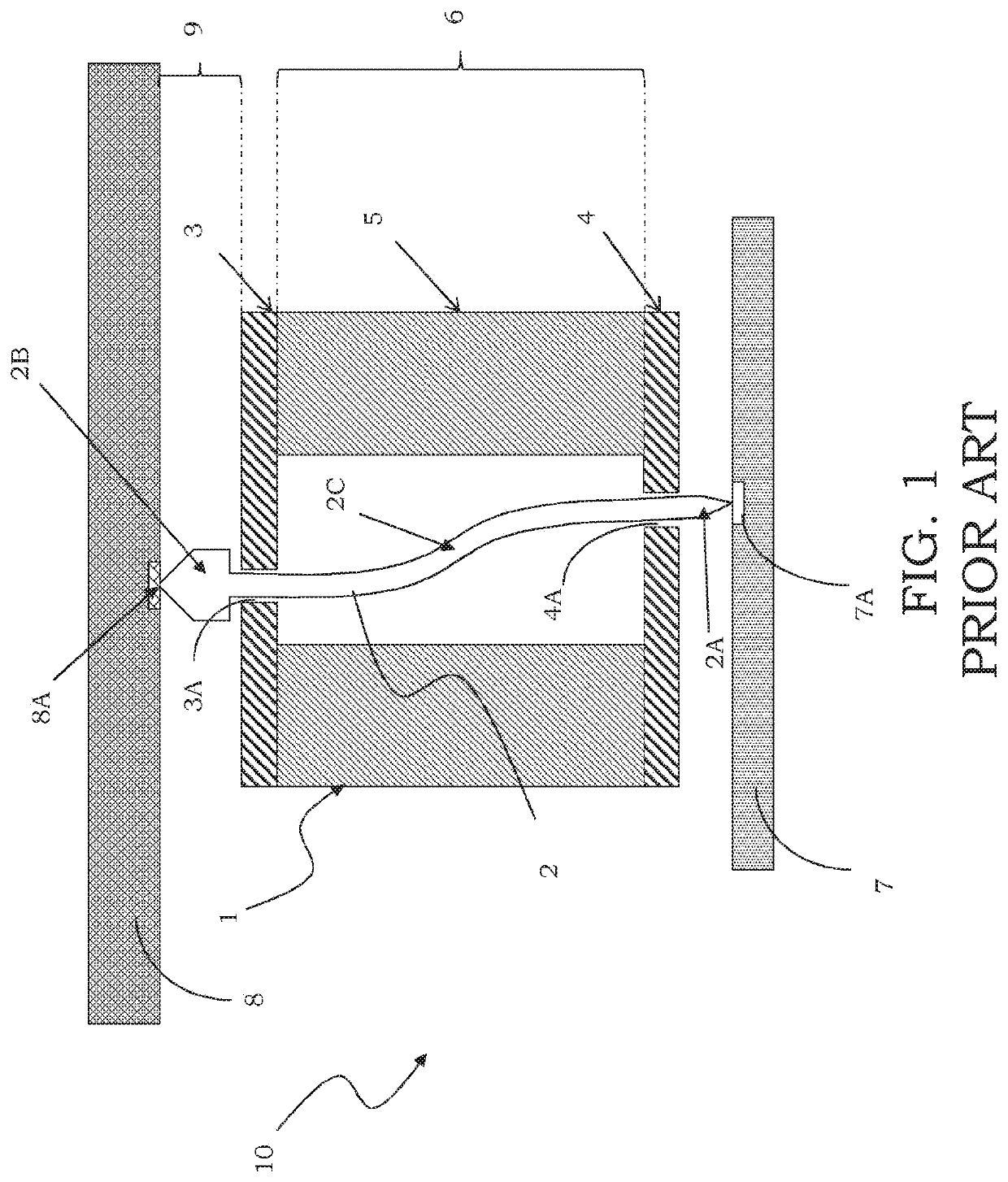
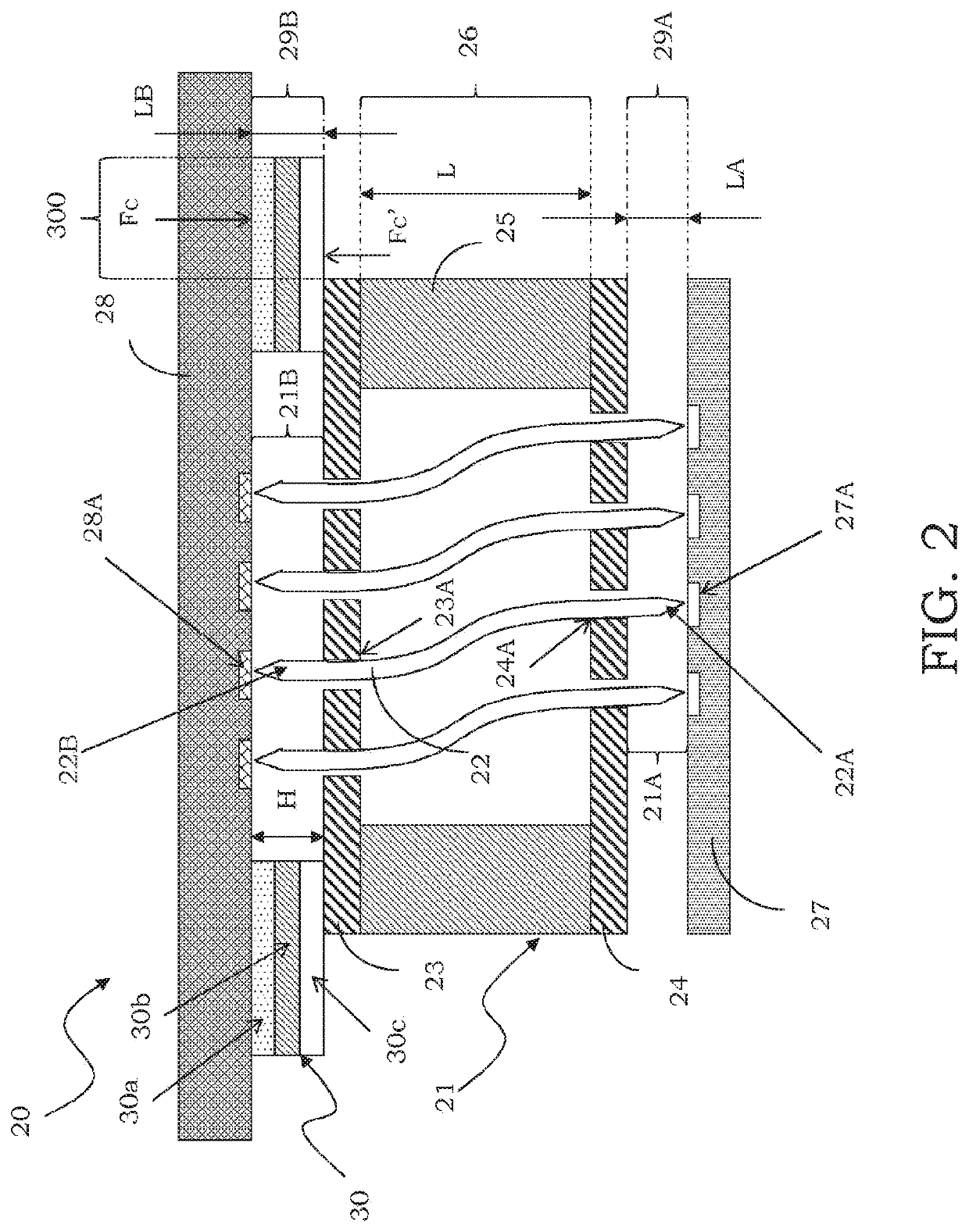
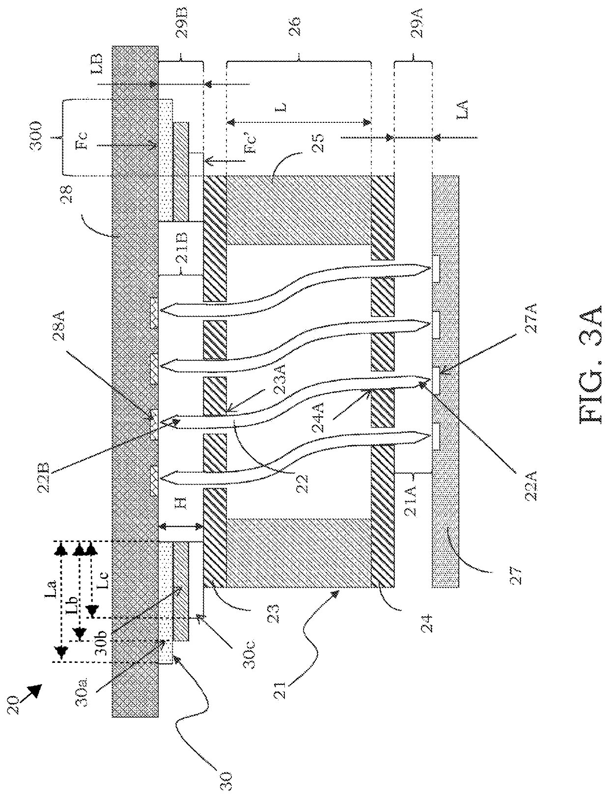
[0067]With reference to such figures, and in particular to FIG. 2, reference 20 globally indicates a probe card realized according to the disclosure.

[0068]It should be noted that the figures are schematic views and are not drawn in scale, but are instead drawn to emphasize the important features of the disclosure. Furthermore it should be noted that arrangements shown with reference to a particular embodiment can obviously be used in combination with other embodiments. Finally, same numeral references are used in the different figures to indicate structurally and functionally corresponding elements.

[0069]The probe card 20 comprises a testing head 21, in turn comprising a plurality of contact probes 22. The testing head also comprises at least one upper guide 23 and a lower guide 24, having respective guide holes 23A and 24A within which the contact probes 2 slide, and is provided with a containment element or case 25 extended between such guides. Between the upper guide 23 and the l...


PUM


Abstract

A probe card for testing of electronic devices comprises a testing head with plural contact probes inserted into guide holes of an upper guide and a lower guide, and a space transformer, each of the contact probes having a first terminal portion projecting from the lower guide with a first length and ending with a contact tip adapted to abut onto a respective contact pad of a device to be tested, and a second terminal portion projecting from the upper guide with a second length and ending with a contact head adapted to abut onto a contact pad of the space transformer. The probe card comprises a spacer element interposed between the space transformer and the upper guide and removable to adjust the first length of the first terminal portion by changing the second length of the second terminal portion and approaching the upper guide and the space transformer.

Description

BACKGROUNDTechnical Field[0001]The present disclosure relates to a probe card for a testing equipment of electronic devices.[0002]The disclosure relates in particular, but not exclusively, to a probe card comprising one testing head with vertical probes for the testing of electronic devices, in particular integrated on wafer and the following description is made with reference to this field of application with the only aim of simplifying its presentation.Description of the Related Art[0003]As is well known, a probe card is essentially a device adapted to put into electrical connection a plurality of contact pads of a microstructure, in particular an electronic device integrated on wafers, with corresponding channels of a testing equipment that performs its functionality check, in particular the electrical one, or generically the testing.[0004]The test performed on integrated devices is particularly useful to detect and isolate flawed devices already in the manufacturing stage. Usual...

Claims


Application Information

Patent Timeline
Patent Type & Authority Patents(United States)
IPC IPC(8): G01R1/073G01R3/00G01R31/28
CPCG01R31/2887G01R3/00G01R1/07357G01R1/07378G01R1/0491G01R1/07314G01R31/2886
Inventor CRIPPA, ROBERTOFELICI, STEFANO
Owner TECHNOPROBE
Why Eureka
Try Eureka