Method for manufacturing organic el device, including a thin film encapsulation structure film-forming method, and film-forming apparatus for the same

a technology of organic el and encapsulation structure, which is applied in the direction of sustainable manufacturing/processing, identification means, instruments, etc., can solve the problems of low mass-productivity, uneven display, and limiting the bendability of the oled display device, so as to improve the mass-productivity and moisture-resistance reliability

Active Publication Date: 2020-08-11
SAKAI DISPLAY PROD
View PDF24 Cites 2 Cited by
  • Summary
  • Abstract
  • Description
  • Claims
  • Application Information

AI Technical Summary

Benefits of technology

[0060]An embodiment of the present invention provides a method for producing an organic EL device that includes a thin film encapsulation structure including a relatively thin organic barrier layer and is improved in the mass-productivity and the moisture-resistance reliability, and a film formation device usable for the method.

Problems solved by technology

An OLED (especially, an organic light emitting layer and a cathode electrode material) is easily influenced by moisture to be deteriorated and to cause display unevenness.
However, such a thick organic barrier layer involves a problem of limiting the bendability of the OLED display device.
There is also a problem that the mass-productivity is low.
Therefore, the element substrate is put into, and out of, a vacuum chamber during the formation of the thin film encapsulation structure, which decreases the mass-productivity.

Method used


Image

  • Method for manufacturing organic el device, including a thin film encapsulation structure film-forming method, and film-forming apparatus for the same
  • Method for manufacturing organic el device, including a thin film encapsulation structure film-forming method, and film-forming apparatus for the same
  • Method for manufacturing organic el device, including a thin film encapsulation structure film-forming method, and film-forming apparatus for the same

Examples


embodiment 1

[0103]With reference to FIG. 3 through FIG. 5, an OLED display device and a method for producing the same according to embodiment 1 of the present invention will be described.

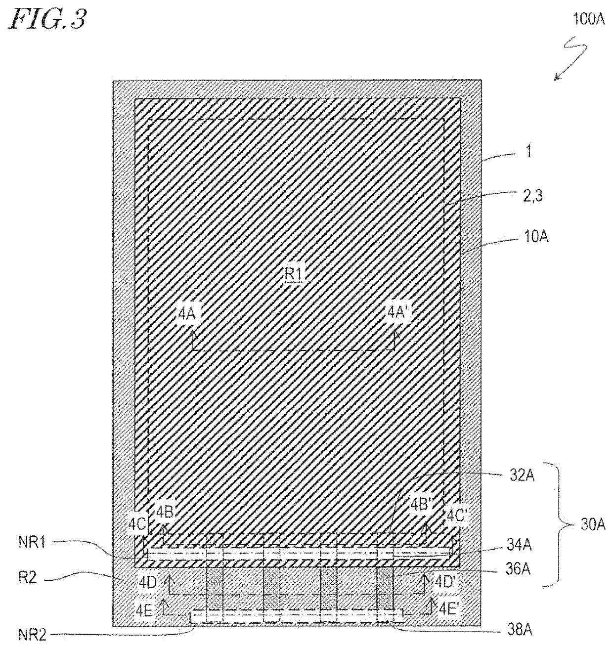
[0104]FIG. 3 is a schematic plan view of an OLED display device 100A according to embodiment 1 of the present invention.

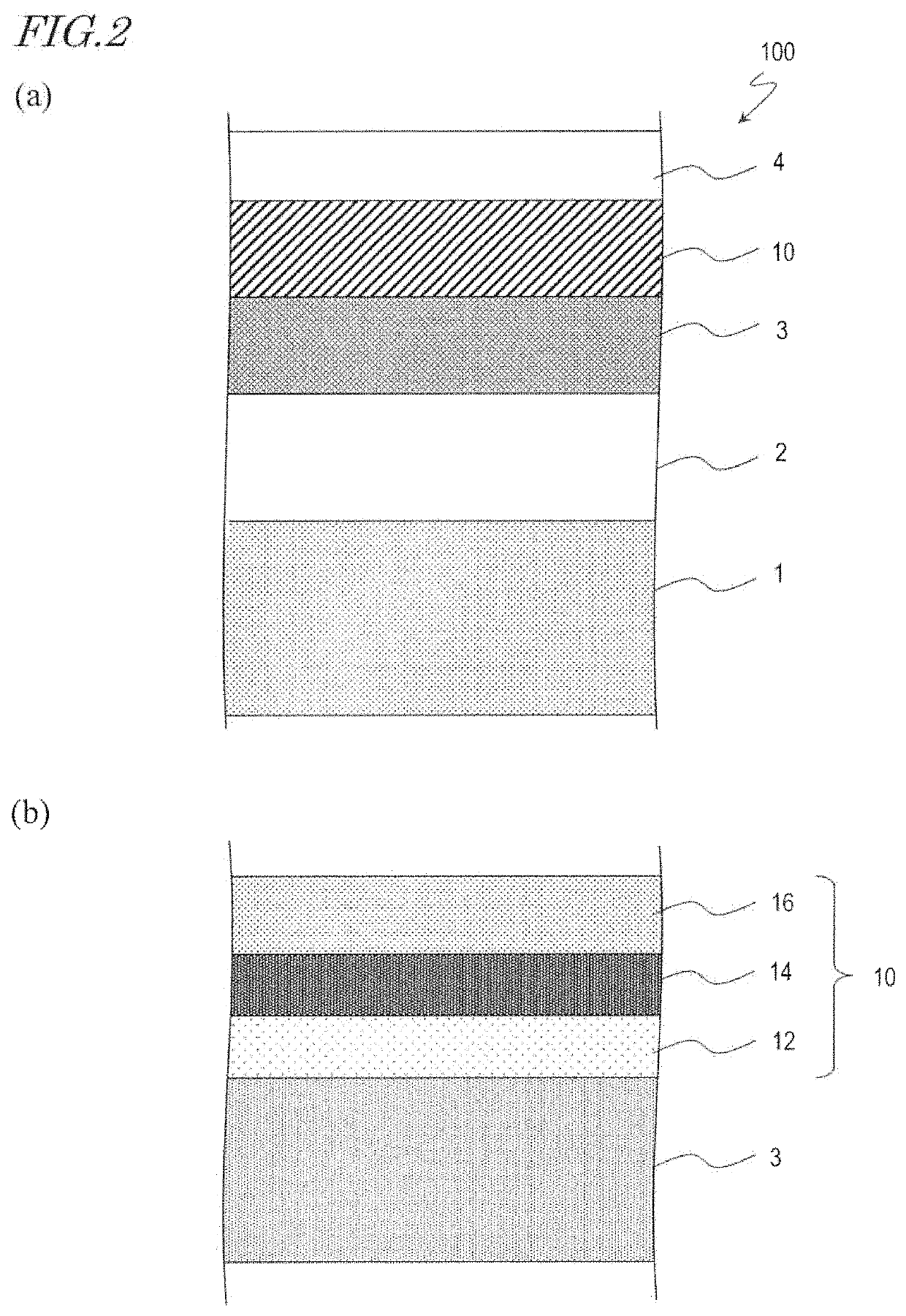
[0105]The OLED display device 100A includes the flexible substrate 1, the circuit (“driving circuit” or “backplane”) 2 formed on the substrate 1, a plurality of the OLEDs 3 formed on the circuit 2, and a TFE structure 10A formed on the OLEDs 3. A layer including the plurality of OLEDs 3 may be referred to as an “OLED layer 3”. The circuit 2 and the OLED layer 3 may share a part of components. The optional polarizing plate (see reference sign 4 in FIG. 2) may further be located on the TFE structure 10A. In addition, for example, a layer having a touch panel function may be located between the TFE structure 10A and the polarizing plate. Namely, the OLED display device 100A may be altered to a di...

embodiment 2

[0217]The method for producing the OLED display device according to embodiment 1, by which the acrylic monomer is located locally, has a problem that the process margin is narrow. A method for producing an OLED display device in embodiment 2 described below includes a step of forming a resin layer (e.g., acrylic resin layer) also at least on a part of the flat portion and partially ashing the resin layer to form an organic barrier layer. The organic barrier layer may be formed in any of various forms by adjusting the thickness of a resin layer to be formed initially (e.g., to less than 100 nm) and / or by adjusting the ashing conditions (including time). Namely, the organic barrier layer 14A included in the OLED display device 100A described in embodiment 1 may be formed, or an organic barrier layer (solid portion) covering a part of, or the entirety of, the flat portion may be formed. The method for producing the OLED display device 100A according to embodiment 1 may be changed such ...


PUM

PropertyMeasurementUnit
wavelengthaaaaaaaaaa
widthaaaaaaaaaa
thicknessaaaaaaaaaa

Abstract

The film-forming method according to an embodiment of the present invention includes: a step A for forming a photocurable resin liquid film on a substrate; a step B for vaporizing the photocurable resin in a first region on the substrate by selectively irradiating the first region with infrared rays or visible light having a wavelength that is longer than 550 nm; and a step C for obtaining a photocured resin film by curing the photocurable resin in the second region on the substrate, said second region including the first region, by irradiating, simultaneously with the step 3 or after performing the step 3, the second region with light, to which the photocurable resin is sensitive.

Description

TECHNICAL FIELD[0001]The present invention relates to a method for producing an organic EL device (e.g., organic EL display device and organic EL illumination device), a film formation method, and a film formation device.BACKGROUND ART[0002]Organic EL (Electroluminescence) display devices start being put into practical use. One feature of an organic EL display device is flexibility thereof. Such an organic EL display device includes, in each of pixels, at least one organic EL element (Organic Light Emitting Diode: OLED) and at least one TFT (Thin Film Transistor) controlling an electric current to be supplied to the at least one OLED. Hereinafter, an organic EL display device will be referred to as an “OLED display device”. Such an OLED display device including a switching element such as a TFT or the like in each of OLEDs is called an “active matrix OLED display device”. A substrate including the TFTs and the OLEDs will be referred to as an “element substrate”.[0003]An OLED (especi...

Claims


Application Information

Patent Timeline
Patent Type & Authority Patents(United States)
IPC IPC(8): H01L51/56H01L27/32H01L51/00H01L51/52
CPCH01L51/0097H01L51/5237H01L51/56H01L27/32H01L51/0001H01L2251/5338H05B33/04H05B33/10G09F9/30Y02E10/549Y02P70/50H10K50/844H10K71/861H10K2102/311H10K71/00H10K50/84H10K59/00H10K77/111
Inventor KISHIMOTO, KATSUHIKO
Owner SAKAI DISPLAY PROD
Why Eureka
Try Eureka