Positioning and fixing device

a technology of positioning and fixing devices, applied in the field of prober, can solve the problems of reducing the position accuracy of the positioning device, the movement mechanism which moves the positioning device, and the unit and the support member (frame) to which the moving mechanism is attached, so as to reduce the increase in the installation area, improve the throughput, and increase the device cost

Active Publication Date: 2020-08-04
TOKYO SEIMITSU
View PDF9 Cites 6 Cited by
  • Summary
  • Abstract
  • Description
  • Claims
  • Application Information

AI Technical Summary

Benefits of technology

[0013]The present invention has been made in view of the above-described circumstances. The present invention aims to provide a prober and a probe inspection method capable of suppressing the increase in installation area and the increase in device cost, and improving the throughput, while maintaining the accuracy of the moving position of the alignment device shared among the measuring units.
[0023]According to the present invention, there is provided the positioning and fixing device, which positions and fixes the alignment device that is moved to each of the measuring units, and hence, it is possible to suppress the increase in installation area and the increase in device cost, and also to improve the throughput while maintaining the accuracy of the moving position of the alignment device.

Problems solved by technology

However, although the testing device described in PTL 1 allows the measuring units to share one alignment device to achieve space saving and cost reduction, the testing device has the following problem.
That is, when the moving distance of the alignment device is increased, a moving mechanism which moves the alignment device to each of the measuring units and a support member (frame) to which the moving mechanism is attached, are easily distorted due to the weight of the alignment device itself and thermal expansion or thermal contraction.
This becomes a cause of reduction of the position accuracy of the alignment device moved to each of the measurement units.
For this reason, much time is taken to detect the positions of the electrode pads and the probes on the wafer by use of imaging means, which results in a problem that the time period for aligning operation is increased, and thereby the throughput becomes low.

Method used


Image

  • Positioning and fixing device
  • Positioning and fixing device
  • Positioning and fixing device

Examples


Embodiment Construction

[0033]In the following, preferred embodiments according to the present invention will be described with reference to the accompanying drawings.

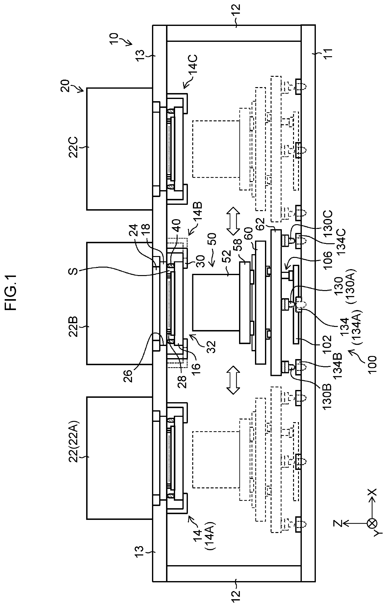
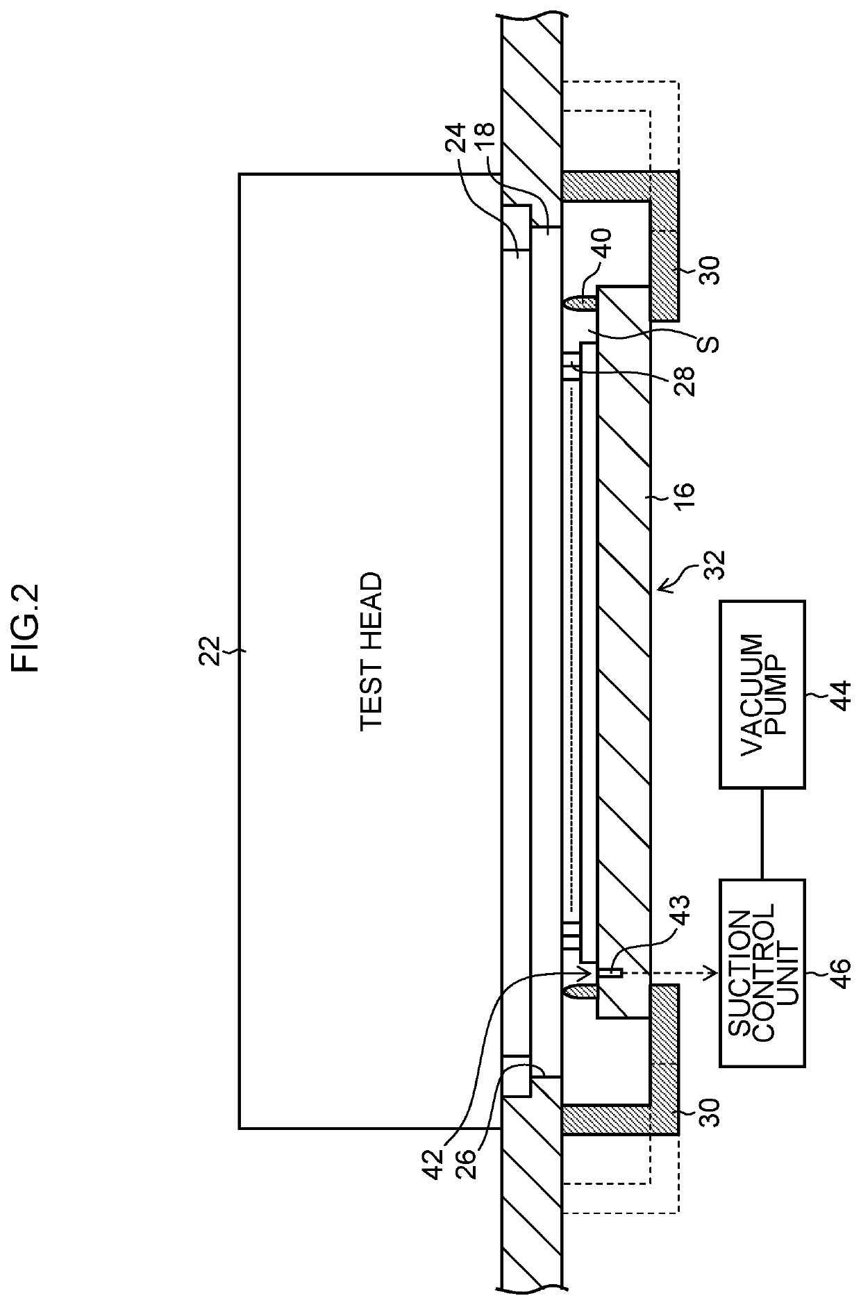
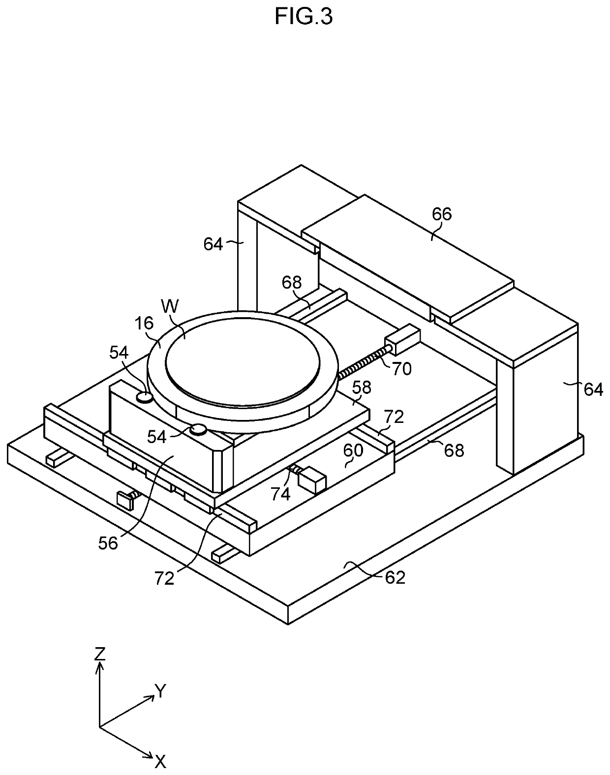
[0034]FIG. 1 shows a schematic configuration of a system which performs wafer level inspection according to an embodiment of the present invention. The system which performs wafer level inspection includes: a prober 10 which brings probes into contact with electrode pads of each of chips on a wafer; and a tester 20 which is electrically connected to the probes and which, for electrical inspection, supplies electric power and test signals to each of the chips and detects output signals from each of the chips to measure whether or not the chips work normally.

[0035]In FIG. 1, the housing of the prober 10 is configured by a base part 11, side plate 12, and a head stage 13. There is also a case where an upper plate supported by the side plate 12 is provided and the head stage 13 is provided on the upper plate.

[0036]The prober 10 is provided with a...


PUM


Abstract

Provided is a prober capable of suppressing the increase in installation area and the increase in device cost, and also improving the throughput, while maintaining the accuracy of the moving position of an alignment device shared by each of measuring units. The prober includes: a plurality of measuring units, each of which has a probe card electrically connected to a test head; a wafer chuck that holds a wafer in which a plurality of chips are formed; an alignment device which performs relative alignment between the probe card and the wafer held by the wafer chuck; a moving device which moves the alignment device among the measuring units; and a positioning and fixing device which is provided for every of the measuring units, and positions and fixes the alignment device which is moved to each of the measuring units.

Description

CROSS-REFERENCE TO RELATED APPLICATIONS[0001]The present application is a Continuation of PCT International Application No. PCT / JP2014 / 071382 filed on Aug. 13, 2014. The above application is hereby expressly incorporated by reference, in its entirety, into the present application.BACKGROUND OF THE INVENTION[0002]Field of the Invention[0003]The present invention relates to a prober for inspecting electrical characteristics of a plurality of semiconductor devices (chips) formed on a semiconductor wafer, and more particularly to a prober in which an alignment device can be shared by a plurality of measuring units, and to a probe inspection method.[0004]Description of the Related Art[0005]In a semiconductor manufacturing process, there are many processes, and in order to improve quality assurance and yield, various inspections are performed in various manufacturing processes. For example, wafer level inspection is performed in such a manner that, in a stage where a plurality of chips fo...

Claims


Application Information

Patent Timeline
Patent Type & Authority Patents(United States)
IPC IPC(8): G01R31/28G01R1/04
CPCG01R31/2891G01R1/0491G01R31/2865
Inventor TAMURA, HIROOTOMOTAKI, KATSURAYOKOYAMA, YOSHIYUKIYOSHIMOCHI, TOMOHIROTAKATORI, MASAMI
Owner TOKYO SEIMITSU
Why Eureka
Try Eureka