Active matrix substrate having plurality of circuit thin film transistors and pixel thin film transistors
a technology of active matrix substrate and circuit thin film transistor, which is applied in the direction of identification means, instruments, semiconductor devices, etc., can solve the problems of difficult reduction (frame-narrowing) of frame area, known technology, etc., and achieve the effect of pixel aperture ratio and light transmittance of active matrix substra
- Summary
- Abstract
- Description
- Claims
- Application Information
AI Technical Summary
Benefits of technology
Problems solved by technology
Method used
Image
Examples
first embodiment
[0044]An active matrix substrate according to a first embodiment of the present invention will be described below with reference to the drawings. The active matrix substrate according to the present embodiment has a monolithic gate driver within a display area. The source driver, for example, is provided in the active matrix substrate, using a COG mounting method.
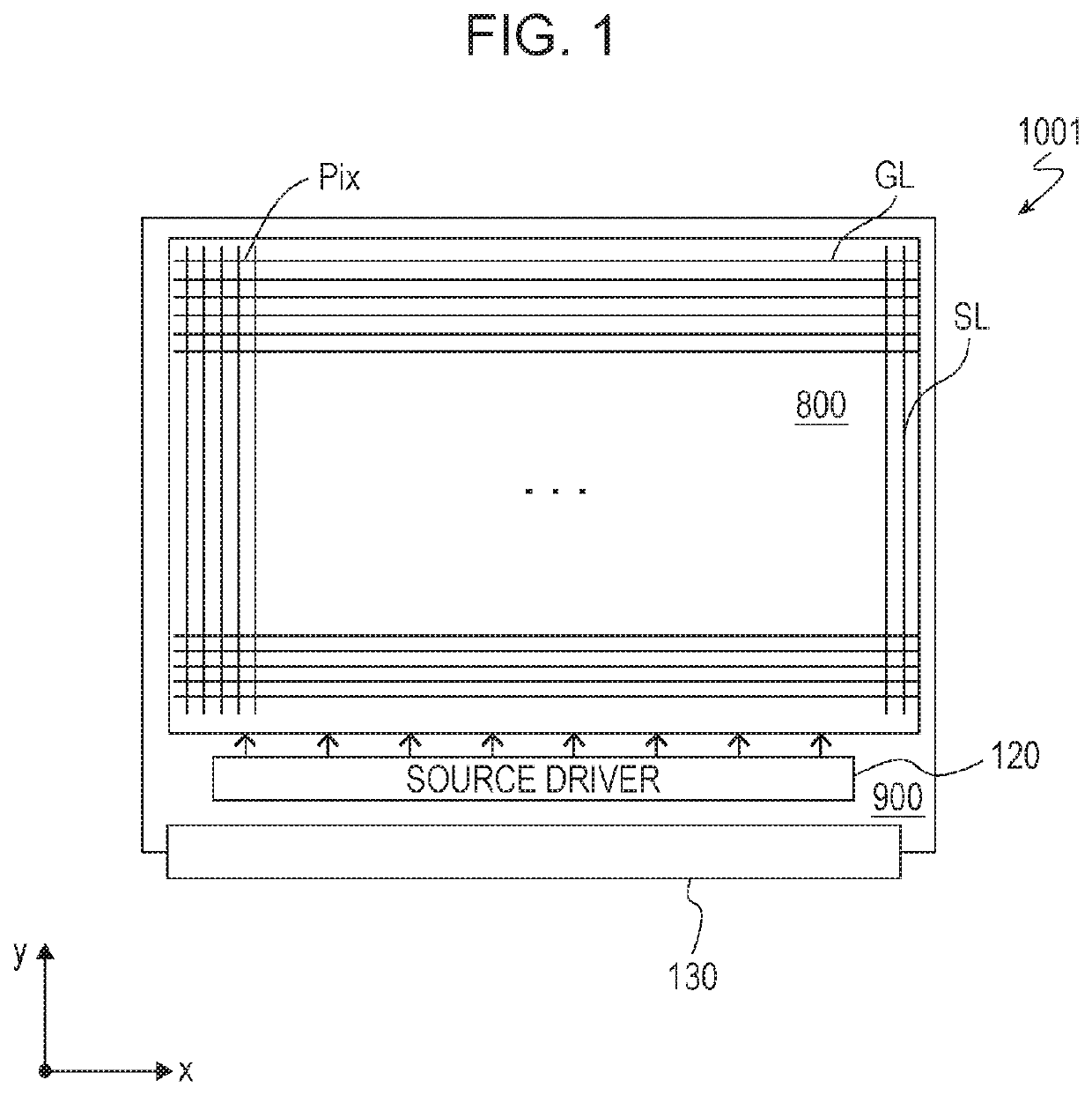
[0045]FIG. 1 is a plan-view diagram illustrating an outline of an active matrix substrate 1001 according to the present embodiment.
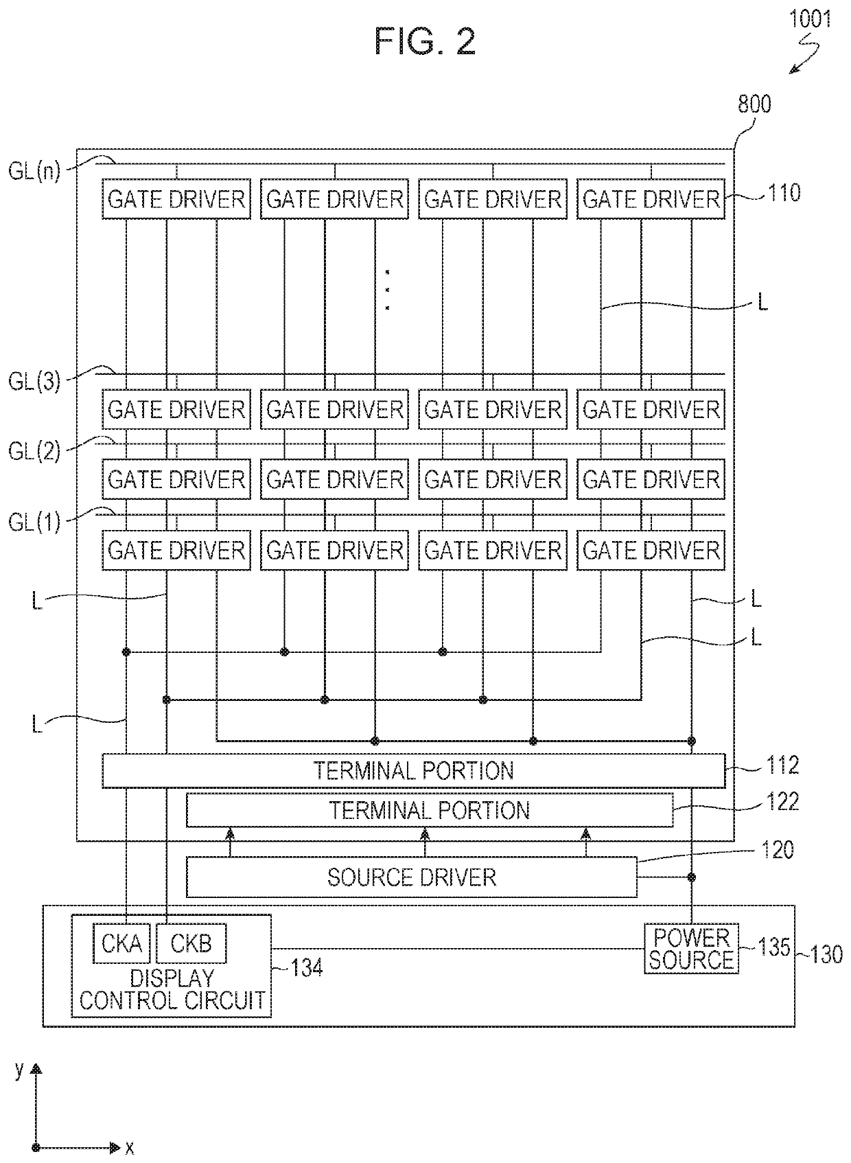
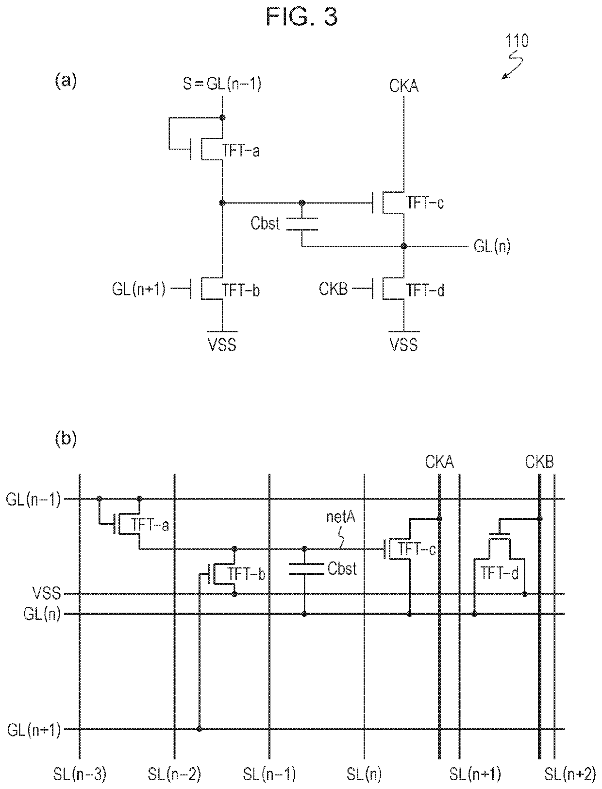
[0046]As illustrated in FIG. 1, the active matrix substrate 1001 includes multiple pixel areas Pix that are arranged in matrix form in a first direction x and a second direction y, multiple gate bus lines GL that extend in the first direction x, and multiple source bus lines SL that extend in the second direction y. An area 800 that includes the multiple pixel areas Pix, of the active matrix substrate 1001 is referred to as “display area”, and an area 900 that is positioned in the vicinity of th...
second embodiment
[0112]An active matrix substrate according to a second embodiment of the present invention will be described below with reference to the drawings. The semiconductor device according to the present embodiment is an active matrix substrate that includes an oxide semiconductor TFT and a crystalline silicon TFT that are formed on the same substrate.
[0113]The active matrix substrate according to the present embodiment includes the first circuit TFT that constitutes a pixel TFT and a drive circuit (for example, a gate driver), in the display area, and includes a second circuit TFT in the non-display area. The second circuit TFT is a circuit TFT that constitutes a peripheral circuit that is monolithically formed in the non-display area. This peripheral circuit may be a Source Shared Driving (SSD) circuit, an inspection circuit, a drive circuit (for example, a source driver), or the like.
[0114]The pixel TFT and the first circuit TFT are oxide semiconductor TFTs that are the same as describe...
third embodiment
[0135]An active matrix substrate according to a third embodiment of the present invention will be described below with reference to the drawings. The semiconductor device according to the present embodiment is an active matrix substrate that includes an oxide semiconductor TFT and a crystalline silicon TFT that are formed on the same substrate.
[0136]A difference from the active matrix substrate 1003 according to the second embodiment is that in the present embodiment, at least a portion of the drive circuit wiring line L is formed using a crystalline silicon film that is the same as the crystalline silicon semiconductor layer 31. Specifically, the drive circuit wiring line L according to the present embodiment includes first and second metal portions that are formed from a gate metal film or a source metal film, and a connection portion that is formed from a crystalline silicon film and that electrically connects the first metal portion and the second metal portion.
[0137]FIG. 10 is ...
PUM
| Property | Measurement | Unit |
|---|---|---|
| thickness | aaaaa | aaaaa |
| thickness | aaaaa | aaaaa |
| thickness | aaaaa | aaaaa |
Abstract
Description
Claims
Application Information
 - R&D
- Intellectual Property
- Life Sciences
- Materials
- Tech Scout
- Unparalleled Data Quality
- Higher Quality Content
- 60% Fewer Hallucinations
Browse by: Latest US Patents, China's latest patents, Technical Efficacy Thesaurus, Application Domain, Technology Topic, Popular Technical Reports.
© 2025 PatSnap. All rights reserved.Legal|Privacy policy|Modern Slavery Act Transparency Statement|Sitemap|About US| Contact US: help@patsnap.com


