Low noise quantized feedback configuration
a quantized feedback and low noise technology, applied in the field of sigmadelta modulators, can solve the problems of adding complexity and cost, and achieve the effect of improving the performance of modulators
- Summary
- Abstract
- Description
- Claims
- Application Information
AI Technical Summary
Benefits of technology
Problems solved by technology
Method used
Image
Examples
Embodiment Construction
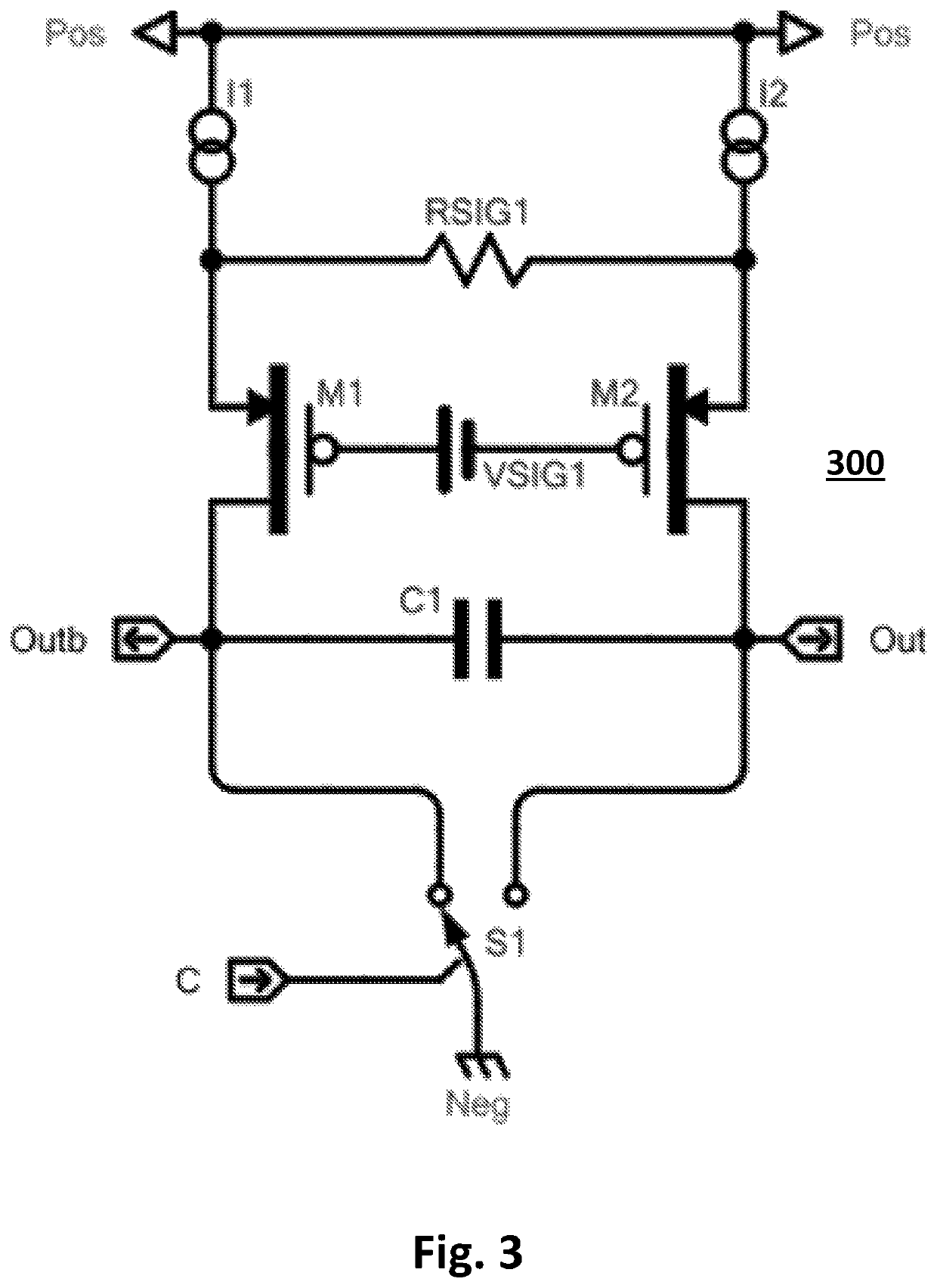
[0017]The present application describes an improved ΣΔ modulator, which may function as an ADC. In one embodiment, the ΣΔ modulator has no common mode control loop, and no reference current. This results in decreased complexity, i.e., fewer components, as well as reduced noise.
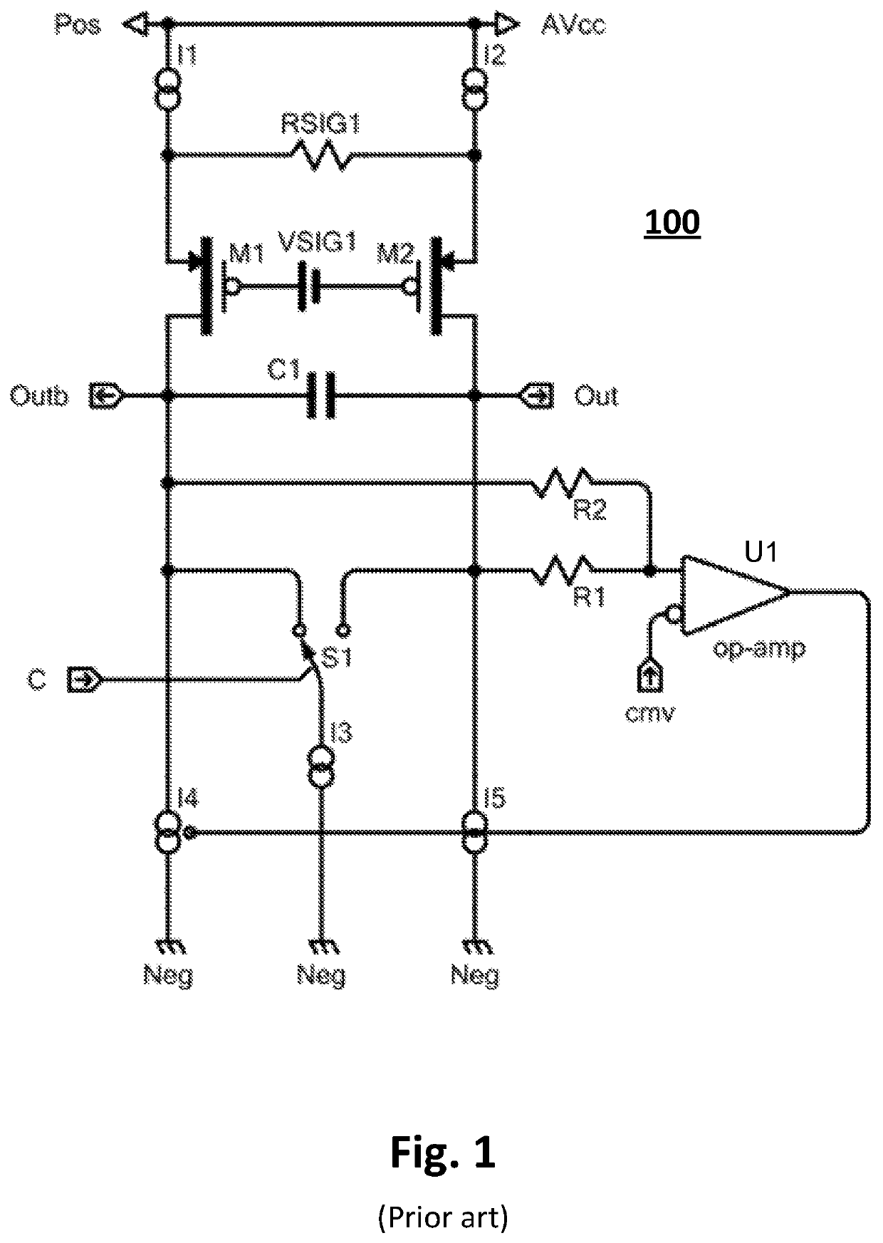
[0018]As explained above, FIG. 1 shows an example of a ΣΔ modulator circuit 100 of the prior art, in which an input difference current is made to flow in the drains of transistors M1 and M2. This occurs because a portion of the nominally equal currents of the current sources I1 and I2 flows through the resistor RSIG1 due to the input voltage VSIG1, which is applied to the gates of transistors M1 and M2.
[0019]This configuration of the upper portion of circuit 100, with current sources I1 and I2, transistors M1 and M2, resistor RSIG1 and an input voltage source VSIG1, is well known to those of skill in the art, and makes what is commonly called a voltage-to-current (V to I) convertor. The V to I convertor conver...
PUM
 Abstract
Description
Claims
Application Information
 - R&D
- Intellectual Property
- Life Sciences
- Materials
- Tech Scout
- Unparalleled Data Quality
- Higher Quality Content
- 60% Fewer Hallucinations
Browse by: Latest US Patents, China's latest patents, Technical Efficacy Thesaurus, Application Domain, Technology Topic, Popular Technical Reports.
© 2025 PatSnap. All rights reserved.Legal|Privacy policy|Modern Slavery Act Transparency Statement|Sitemap|About US| Contact US: help@patsnap.com


