Split-gate non-volatile memory and fabrication method thereof

a technology of non-volatile memory and split-gate, which is applied in the field of split-gate non-volatile memory and a fabrication method thereof, can solve problems such as poor data retention, and achieve the effects of erasing the gate, improving data retention, and reducing leakage curren

Active Publication Date: 2020-04-28
NEXCHIP SEMICON CO LTD
View PDF2 Cites 0 Cited by
  • Summary
  • Abstract
  • Description
  • Claims
  • Application Information

AI Technical Summary

Benefits of technology

[0003]In view of the above-mentioned disadvantages of the prior art, the purpose of the present invention is to provide a split-gate non-volatile memory and a fabrication method thereof, which are used for solving the problems that, since the thickness of the tunneling dielectric layer in the split-gate memory in the prior art is relatively small in order to guarantee erasing, current leakage is easily caused and consequently the problem of poor data retention of the memory is caused.
[0064]As described above, the split-gate non-volatile memory and fabrication method thereof provided by the present invention have the following beneficial effects: by designing the top portion of the floating gate to be the sharp tip, the FN tunneling effect between the floating gate and the erasing gate can be obviously increased; since the top portion of the floating gate is the sharp tip, the thickness of the tunneling dielectric layer between the erasing gate and the floating gate can be increased, thus leakage current is avoided and the split-gate non-volatile memory is enabled to have better data retention.

Problems solved by technology

However, a material of the existing tunneling dielectric layer is generally silicon oxide or silicon nitride, but silicon oxide and silicon nitride are not complete insulators, when the thickness of the tunneling dielectric layer is small, leakage current is very easily caused, charges stored in the floating gate leak into the erasing gate and are erased, and consequently the problem of poor data retention is caused.

Method used


Image

  • Split-gate non-volatile memory and fabrication method thereof
  • Split-gate non-volatile memory and fabrication method thereof
  • Split-gate non-volatile memory and fabrication method thereof

Examples


embodiment 1

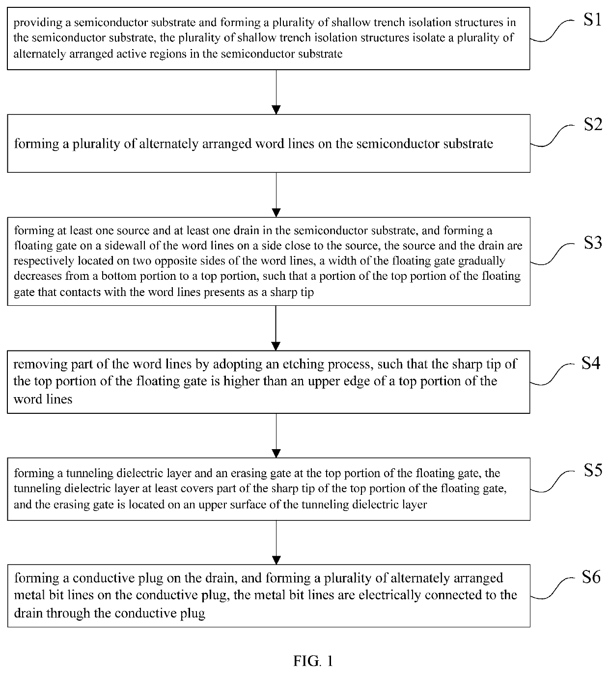
[0119]Please refer to FIG. 1, the present invention provides a method for fabricating a split-gate non-volatile memory. The method for fabricating the split-gate non-volatile memory comprises the following steps:

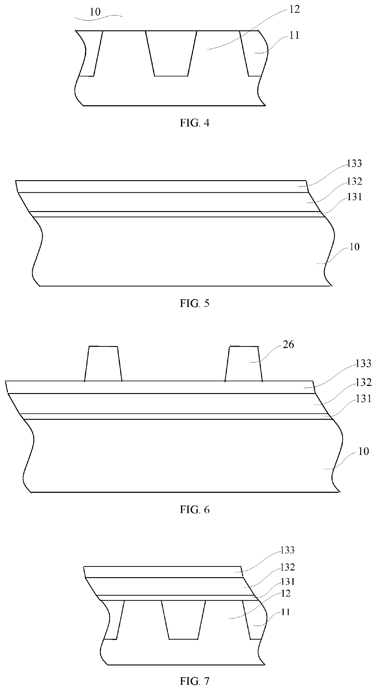
[0120]1) providing a semiconductor substrate and forming a plurality of shallow trench isolation structures in the semiconductor substrate, wherein the plurality of shallow trench isolation structures isolate a plurality of spaced active regions in the semiconductor substrate;

[0121]2) forming a plurality of spaced word lines on the semiconductor substrate;

[0122]3) forming at least one source and at least one drain in the semiconductor substrate, and forming a floating gate on a sidewall of the word lines on a side close to the source, wherein the source and the drain are respectively located on two opposite sides of the word lines, a longitudinal section width of the floating gate gradually decreases from a bottom portion to a top portion such that a portion of the top porti...

embodiment 2

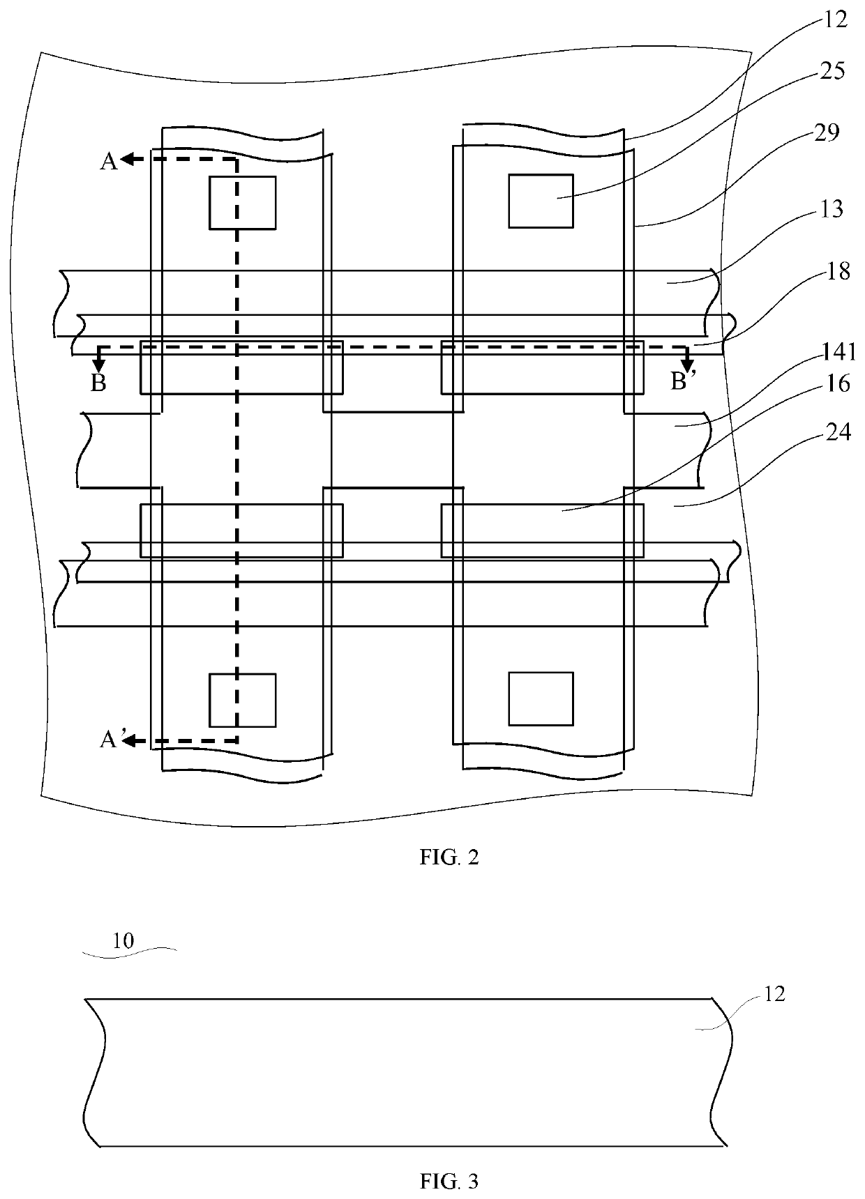
[0180]In combination with FIG. 2 to FIG. 25, continuously refer to FIG. 26 to FIG. 27, the present invention further provides a split-gate non-volatile memory. The split-gate non-volatile memory may be obtained by adopting, but not limited to, the method for fabricating the split-gate non-volatile memory in embodiment 1. The split-gate non-volatile memory at least comprises: a semiconductor substrate 10, a plurality of shallow trench isolation structures 11 are formed in the semiconductor substrate 10, the shallow trench isolation structures 11 isolate a plurality of spaced active regions 12 in the semiconductor substrate 10; a plurality of spaced word lines 13; a source 14; a drain 15, the source 14 and the drain 15 are respectively located on two opposite sides of the word lines 13; a floating gate 16 located on a sidewall of the word lines 13 close to the source 14, a longitudinal section width of the floating gate 16 gradually decreases from a bottom portion to a top portion suc...


PUM

PropertyMeasurementUnit
angleaaaaaaaaaa
thicknessaaaaaaaaaa
thicknessaaaaaaaaaa

Abstract

A split-gate non-volatile memory and a fabrication method thereof. The method comprises the following steps: 1) forming a plurality of shallow trench isolation structures in a semiconductor substrate; 2) forming word lines on the semiconductor substrate; 3) forming a source and a drain in the semiconductor substrate, and forming a floating gate on a sidewall of the word line on a side close to the source, a portion of the floating gate that contacts with the word lines presents as a sharp tip; 4) removing part of the word lines by adopting an etching process such that the sharp tip of the top portion of the floating gate is higher than the word lines; 5) forming a tunneling dielectric layer and an erasing gate at the top portion of the floating gate; and 6) forming a conductive plug on the drain and forming metal bit lines on the conductive plug.

Description

BACKGROUND OF THE PRESENT INVENTIONField of Invention[0001]The present invention relates to the technical field of semiconductors, in particular to a split-gate non-volatile memory and a fabrication method thereof.Description of Related Arts[0002]In the existing split-gate memories, since a tunneling effect between a floating gate and an erasing gate is limited, in order to facilitate implementing quick erasing under a situation of small power, a thickness of a tunneling dielectric layer between the floating gate and the erasing gate is generally small. However, a material of the existing tunneling dielectric layer is generally silicon oxide or silicon nitride, but silicon oxide and silicon nitride are not complete insulators, when the thickness of the tunneling dielectric layer is small, leakage current is very easily caused, charges stored in the floating gate leak into the erasing gate and are erased, and consequently the problem of poor data retention is caused.SUMMARY OF THE PR...

Claims


Application Information

Patent Timeline
Patent Type & Authority Patents(United States)
IPC IPC(8): H01L29/792H01L27/11521H01L27/11519H01L21/28H01L21/768H01L21/762H01L29/423
CPCH01L29/42328H01L21/76897H01L29/40114H01L27/11521H01L21/76224H01L27/11519H10B41/30H10B41/10
Inventor CHERN, GEENG-CHUAN
Owner NEXCHIP SEMICON CO LTD
Why Eureka
Try Eureka