
Light-emitting device and lighting system comprising same

a technology of light-emitting devices and lighting systems, which is applied in the direction of semiconductor devices, lighting and heating apparatus, light sources, etc., can solve problems such as energy band bending, and achieve the effects of reducing energy band bending, reducing leakage of carrier components, and improving hole injection efficiency

Active Publication Date: 2019-12-17
SUZHOU LEKIN SEMICON CO LTD
View PDF18 Cites 0 Cited by
  • Summary
  • Abstract
  • Description
  • Claims
  • Application Information

AI Technical Summary

Benefits of technology

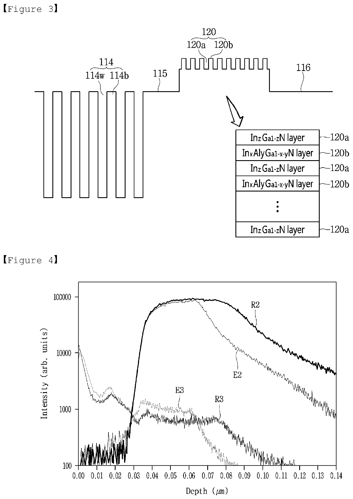
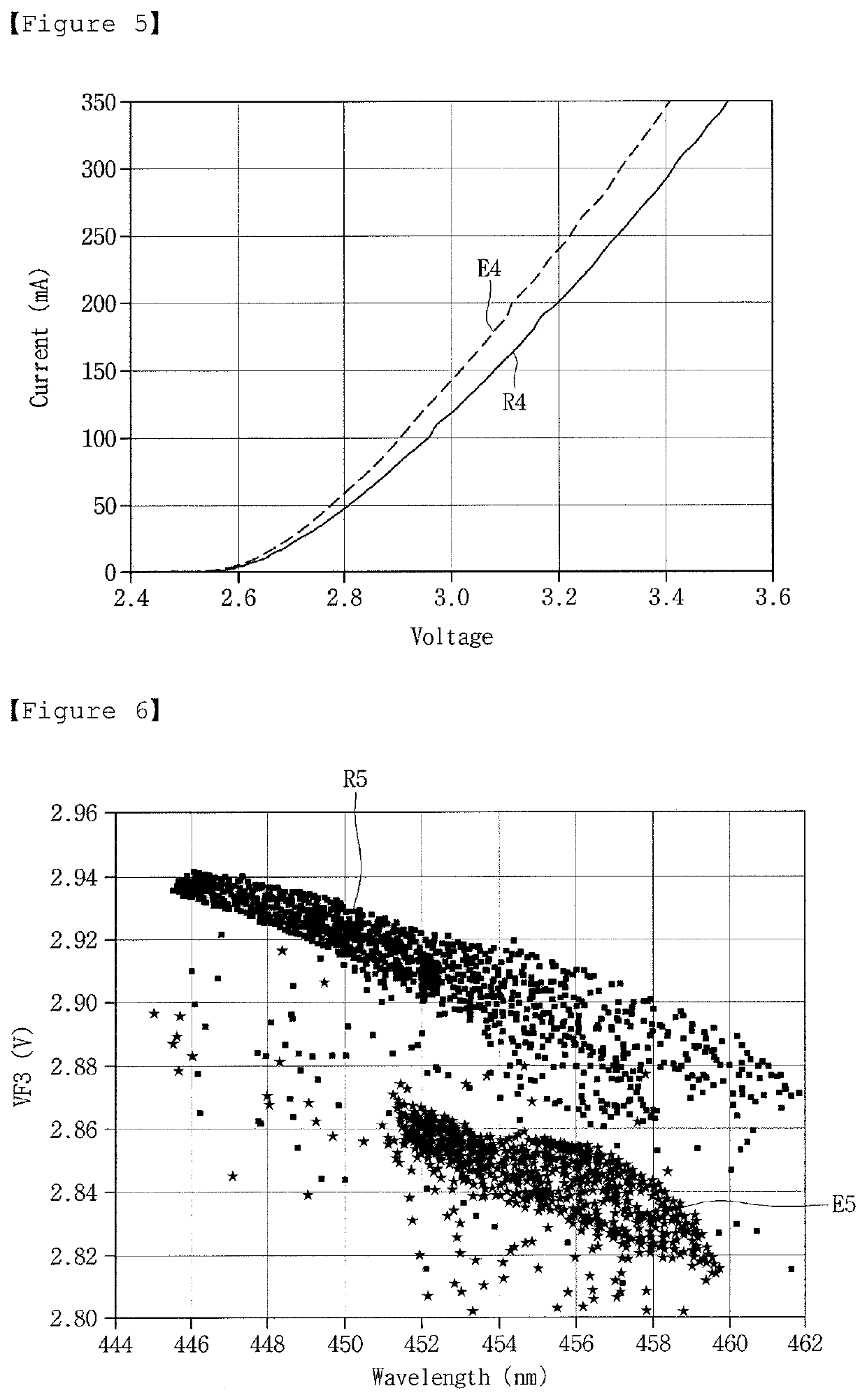
[0010]According to the embodiment, hole injection efficiency may be improved by decreasing the bending of an energy band in a valance band.
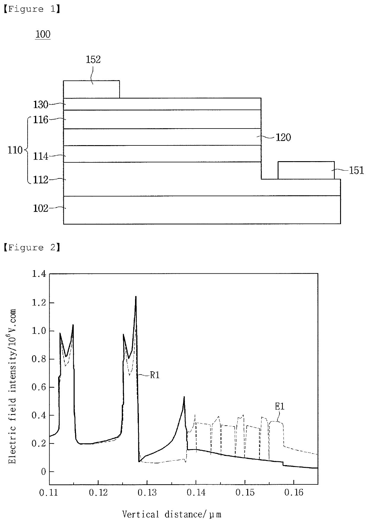
[0011]According to the embodiment, carrier leakage can be minimized by reducing the electrostatic field between the active layer and the electron blocking layer.

Problems solved by technology

However, as the stress occurs due to the lattice mismatch between a barrier of an active layer and the electron blocking layer, the energy band is bent.

Method used


Image

  • Light-emitting device and lighting system comprising same
  • Light-emitting device and lighting system comprising same
  • Light-emitting device and lighting system comprising same

Examples


Embodiment Construction

[0021]In the description of the embodiment, it will be understood that, when a layer (or film), an area, a pattern, or a structure is referred to as being “on” or “under” a substrate, each layer (or film), each area, each pad, or patterns, it can be “directly” or “indirectly” over the substrate, or the layer (or film), area, pad, or pattern, or one or more intervening layers may also be present. Such a position of the layer has been described with reference to the drawings.

[0022]FIG. 1 is a sectional view of a light emitting device according to the embodiment.

[0023]Referring to FIG. 1, according to the embodiment, a light emitting device 100 may include a substrate 102, a light emitting structure 110 including a first conductive-type semiconductor 112 on the substrate 102, an active layer 114 on the first conductive-type semiconductor 112, a second conductive-type semiconductor layer 116 on the active layer 114, and an electron blocking layer 120 disposed between the active layer 11...


PUM


Abstract

Embodiments relate to a light emitting device, a light emitting device package, and a lighting system comprising the same. The light emitting device according to embodiments may comprise: a first conductivity-type semiconductor layer; an active layer on the first conductivity-type semiconductor layer; an electron blocking layer on the active layer; and a second conductivity-type semiconductor layer on the electron blocking layer. The electron blocking layer may comprise an InxAlyGa1-x-yN based superlattice layer (wherein 0≤x≤1, 0≤y≤1).

Description

CROSS REFERENCE TO RELATED APPLICATIONS[0001]This application is the National Phase of PCT International Application No. PCT / KR2016 / 001421, filed on Feb. 12, 2016, which claims priority under 35 U.S.C. 119(a) to Patent Application No. 10-2015-0023144, filed in the Republic of Korea on Feb. 16, 2015, all of which are hereby expressly incorporated by reference into the present application.TECHNICAL FIELD[0002]The embodiment relates to a light emitting device, a light emitting device package including the same, and a lighting system including the same.BACKGROUND ART[0003]A light emitting diode (LED) includes a P-N junction diode having a characteristic of converting electric energy into light energy, and may be formed by using compound semiconductors of group III-V elements on the Periodic Table. In addition, the LED may represent various colors realized by adjusting the compositional ratio of the compound semiconductors[0004]When forward voltage is applied to the LED, electrons of an ...

Claims


Application Information

Patent Timeline
Patent Type & Authority Patents(United States)
IPC IPC(8): H01L33/14F21K9/232F21K9/235H01L33/04H01L33/32F21K9/237H01L33/02H01L33/06F21Y115/10
CPCH01L33/04F21K9/235H01L33/32H01L33/06H01L33/025F21K9/232F21K9/237H01L33/145F21Y2115/10H01L33/0075
Inventor HAN, YOUNG HUN
Owner SUZHOU LEKIN SEMICON CO LTD
Learn More