Photogate for front-side-illuminated infrared image sensor and method of manufacturing the same

a technology of infrared image sensor and photogate, which is applied in the field of image sensor, can solve the problems of increasing increasing the difficulty in producing an image sensor that produces both high-quality color and infrared images, and increasing the complexity of image sensors used in the above applications, so as to reduce the risk of poor-performing pixels, improve pixel sensitivity, and reduce the effect of dark curren

Active Publication Date: 2019-12-10
OMNIVISION TECH INC
View PDF2 Cites 3 Cited by
  • Summary
  • Abstract
  • Description
  • Claims
  • Application Information

AI Technical Summary

Benefits of technology

[0009]The present invention overcomes the problems associated with the prior art, by providing a front-side-illuminated image sensor that includes infrared pixels for detecting infrared light, where each infrared pixel includes a photogate formed over a light-sensitive region. The infrared pixels can also include deep infrared detecting regions that extend into one or more neighboring color pixel(s). The infrared pixel design of the invention reduces dark current, improves pixel sensitivity, and increases full-well capacity of the infrared pixels.

Problems solved by technology

Image sensors used in the above applications continue to become more complex to meet required demands.
These color and infrared pixels have different structural and performance requirements, which results in difficulties producing an image sensor that produces both high-quality color and infrared images.
Unfortunately, the risk of poor-performing pixels increases as more implants are made, because the implantation equipment deposits metal contaminants (e.g., titanium (Ti), tungsten (W), etc.) in the substrate.
Excessive dark current is particularly problematic for infrared pixels, because infrared pixels are used to capture images in the dark.
Metal contamination caused by ion implantation equipment is a major cause of dark current.
Another problem associated with image sensors is charge saturation.
Early saturation of a photodetector is undesirable, because its sensitivity is reduced (e.g., it will indicate a full bright pixel earlier) compared to a photodetector that does not prematurely saturate.
Thus, low well capacity and saturation can be problematic in infrared sensors used in dark environments, especially when too many bright pixels result in the final image.
Another difficulty with infrared pixel design results because infrared light is detected deep in the silicon substrate as compared to shorter wavelengths of (visible) light.
Therefore, transferring the accumulated infrared charge from deep in the silicon substrate to read-out circuitry can be difficult for infrared pixels.

Method used


Image

  • Photogate for front-side-illuminated infrared image sensor and method of manufacturing the same
  • Photogate for front-side-illuminated infrared image sensor and method of manufacturing the same
  • Photogate for front-side-illuminated infrared image sensor and method of manufacturing the same

Examples


Embodiment Construction

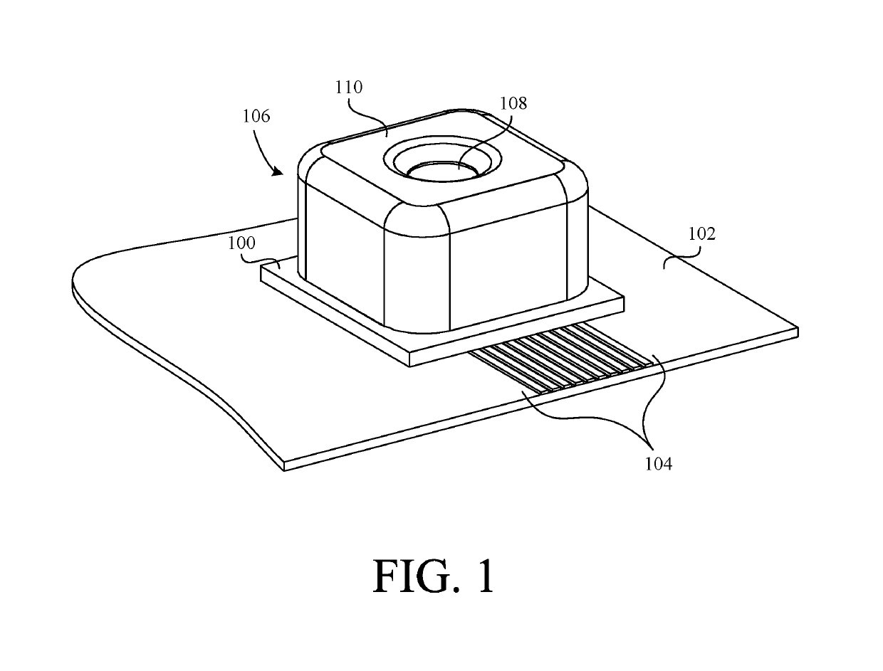
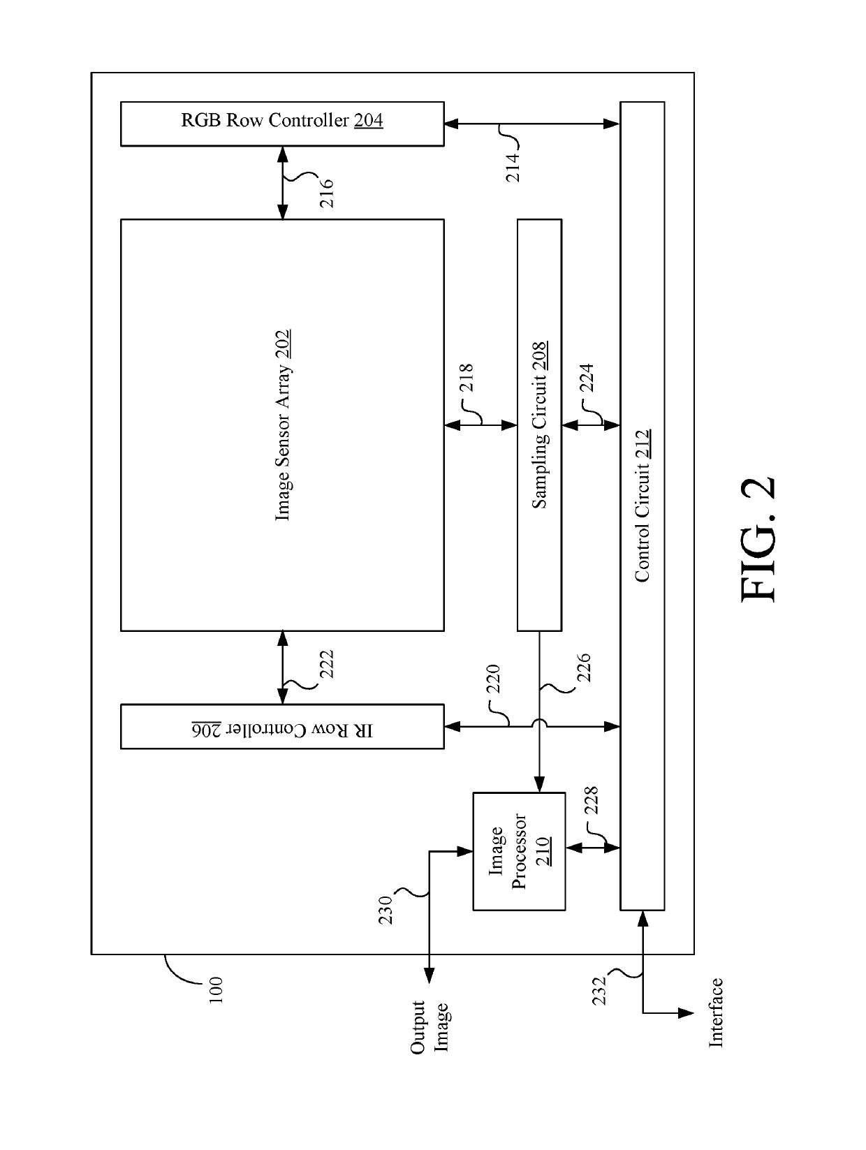
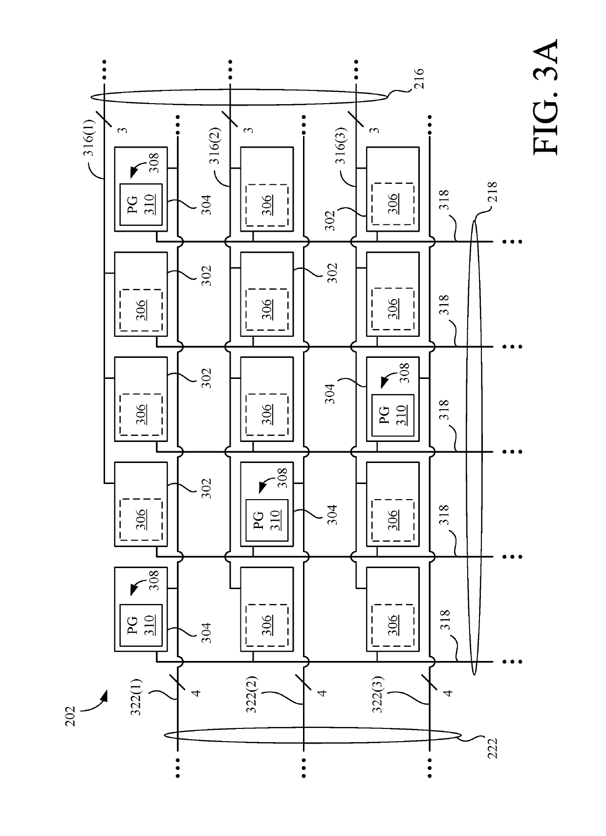
[0030]The present invention overcomes the problems associated with the prior art, by providing a front-side-illuminated image sensor having infrared pixels, each of which includes a photogate that improves the pixel's performance, in part by reducing the number of substrate implants. The infrared pixels can also include a deep charge-accumulation region that underlies neighboring color pixel(s) and improves the sensitivity of the infrared pixels. In the following description, numerous specific details are set forth (e.g., particular types of doping, particular pixel layouts, etc.) in order to provide a thorough understanding of the invention. Those skilled in the art will recognize, however, that the invention may be practiced apart from these specific details. In other instances, details of well-known image sensor design and semiconductor fabrication practices (e.g., metallization, photo-masking, routine optimization, etc.) and components have been omitted, so as not to unnecessari...


PUM


Abstract

An image sensor includes a substrate and a plurality of infrared pixels formed in a front side of the substrate and configured to detect infrared light incident on the front side of the substrate. Each of the infrared pixels includes a photodiode, a region free of implants located above the photodiode, and a photogate formed over the substrate and above the photodiode. The image sensor also includes a plurality of color pixels dispersed among the infrared pixels, where each of the color pixels includes a pinned photodiode and is configured to detect visible light. The photodiode of each of the infrared pixels can include a deep charge-accumulation region underlying the pinned photodiode(s) of one or more neighboring color pixel(s). Methods of manufacturing also described and include forming the deep charge-accumulation regions and associated elements prior to forming any implant-blocking elements (e.g., polysilicon photogates) over the substrate.

Description

BACKGROUND OF THE INVENTIONField of the Invention[0001]This invention relates generally to image sensors that detect infrared light, and more particularly to a front-side-illuminated (FSI) image sensor that includes photogates for pixels that detect infrared light but not for pixels that detect visible light.Description of the Background Art[0002]Electronic image sensors are commonly incorporated into a variety of host devices including, for example, cell phones, computers, digital cameras, PDA's, etc. In addition to conventional user-controlled still and video camera applications, more and more image sensor applications are emerging. For example, integral machine vision applications are expanding rapidly in the automotive, manufacturing, medical, security, and defense industries. In such applications, machines perform certain operational tasks (e.g. collision prevention) based at least in part on information received from its image sensor(s). For the machine to properly perform its...

Claims


Application Information

Patent Timeline
Patent Type & Authority Patents(United States)
IPC IPC(8): H01L27/146H01L31/105H01L31/113
CPCH01L31/1136H01L27/14649H01L31/105H01L27/14645
Inventor GOTO, TAKAYUKIYANG, DAJIANGMABUCHI, KEIJIMANABE, SOHEI
Owner OMNIVISION TECH INC
Why Eureka
Try Eureka