Photoconversion of light using metal supported atomic quantum clusters

a technology of atomic quantum clusters and photoconversion, which is applied in the field of metal nanoparticles, can solve the problems of reducing efficiency, no general agreement of how some factors behave, and low photocatalytic and photovoltaic properties

Active Publication Date: 2019-11-05
UNIVERSITY OF SANTIAGO DE COMPOSTELA
View PDF12 Cites 2 Cited by
  • Summary
  • Abstract
  • Description
  • Claims
  • Application Information

AI Technical Summary

Benefits of technology

[0012]The inventors of the present invention have found that Atomic Quantum Clusters (AQCs) can be used as semiconductors for light harvesting. Using AQCs supported on metal nanoparticles having equal or very similar Fermi levels, the electrons and holes generated after light irradiation can be easily separated without almost any recombination. In the case of using AQC semiconductor clusters of the same material than the supporting metal, the Fermi levels of both are equal. Therefore, in principle, an Ohmic contact will be formed at the interface. As the AQCs have such a small size, all the surface of the AQCs attached to the metal nanoparticles is considered to be in the interface AQC / nanoparticle and, therefore, all the excitons (hole-electron pairs) are formed at the interface. This fact implies an increase of interface area, a higher interfacial charge-carrier transfer rate and a decrease of the recombination probabilities, and therefore an increase in the efficacy of the semiconductor of the invention, i.e. the AQCs, compared to the traditional semiconductors known in the art, e.g. TiO2, ZnO, CdS, etc.

Problems solved by technology

Efficient charge separation after photon absorption by a semiconductor (SC) is one of the main challenges in the efficient harvesting of light energy.
Although some of these factors can be controlled to improve the performances, there is no general agreement of how some of the factors behave.
However, the rapid surface hole-electron recombination in nanoparticles makes that the photocatalytic and photovoltaic properties are lower than their larger counterpart.
Another important interfacial problem, mainly related with photovoltaic applications, is due to the poor interaction at the solid / solid junction, i.e. the interface between the semiconductor and the metals used for driving the current, reducing the efficiency.
The necessity of a good Ohmic contact at the semiconductor-metal interface as carrier collection is very inefficient when this interface is non-Ohmic, because such non-Ohmic contacts lead to higher overpotentials to attain a given anodic current.
Overcoming such difficulty requires the use of intermediate layers / coatings to improve such interaction, but in any case, the efficiency is largely reduced.

Method used


Image

  • Photoconversion of light using metal supported atomic quantum clusters
  • Photoconversion of light using metal supported atomic quantum clusters
  • Photoconversion of light using metal supported atomic quantum clusters

Examples


example 1

Photodissolution of Gold Nanorods

a) Preparation of Au Nanorods Containing Clusters:

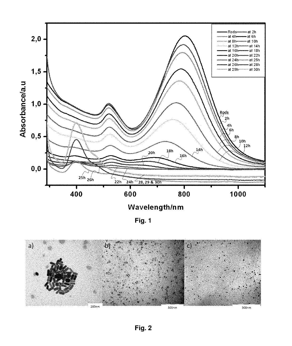
[0169]Firstly, a seed solution was prepared as follows: 2.5 ml of 0.2 M CTAB (cetyltrimethylammonium bromide, (C16H33)N(CH3)3Br) solution was mixed with 2.5 ml of 5×10⁻⁴ M HAuCl4. To the stirred solution, 30 μl of ice-cold 0.1M NaBH4 was added, which results in the formation of a solution with brownish yellow color. Vigorous stirring of the seed solution was continued for 2 minutes. We then used this seed solution 10 minutes after the addition of the reducing agent. Then, a growth solution was prepared as follows: 0.1 ml of 4×10⁻³ M AgNO3 solution was added to 2.5 ml of 0.2 M CTAB. To this solution, 2.5 ml of 10−3 M HAuCl4 was added and, after gentle mixing of the solution, 35 μl of 0.0788 M ascorbic acid was added. Ascorbic acid, as a reducing agent, changes the growth solution from dark yellow to colorless within 10 minutes. The final step was the addition of the seed solution to the growth solution...

example 2

Stability of Clusters Against Irradiation

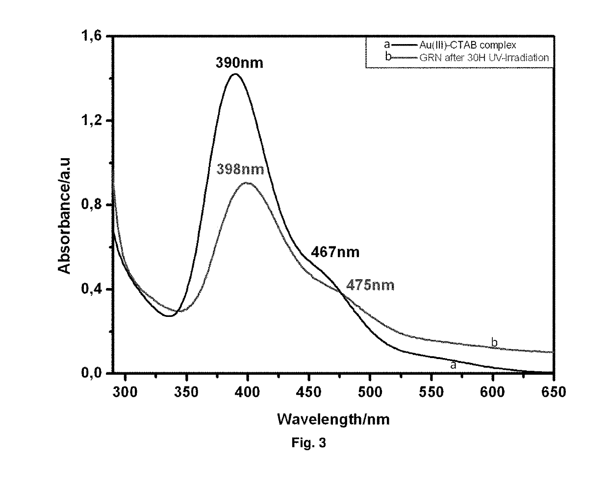
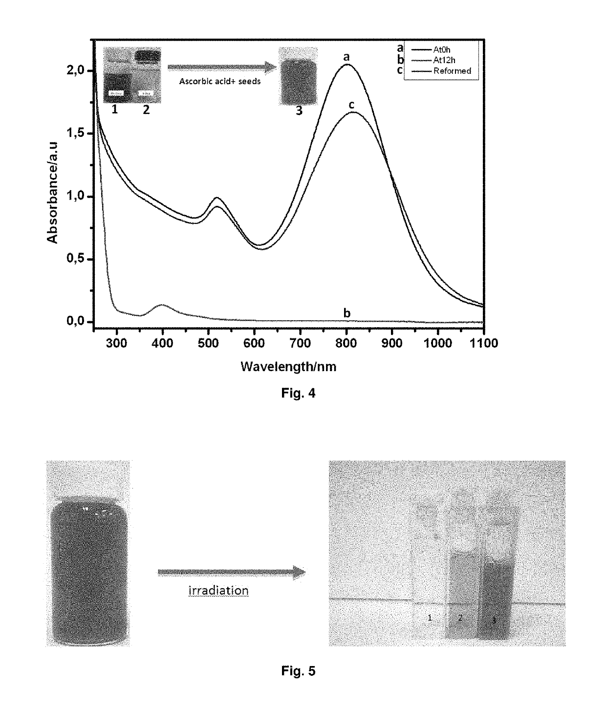
[0171]Contrary to what happens with many semiconductors, which are dissolved by photocorrosion after being irradiated for some periods of time, the semiconductor Ag clusters remain active after complete dissolution of the metal gold NRs, as it can be shown in FIG. 4, which shows that, after the dissolution of a sample of Au NRs, (as it was indicated in Example 1b), just adding new reactants (ascorbic acid and seeds), without Ag salt—which was used to form the Ag clusters catalyzing the formation of Au NRs before irradiation-, to the final sample obtained after irradiation, the re-formation of Au NRs is observed.

example 3

Inhibition of Photocorrosion by Pre-Heating the Au NRs Samples

[0172]To further show that clusters are responsible for the photocorrosion of the Au NRs, an experiment was done just heating the solution of gold NRs prepared according to the Example 1a) at high temperatures. As it was shown in the patent application WO 2011 / 064430, unsupported AQCs fuse at temperatures in the range of 120-150° C. Therefore, if gold NRs are heated at those temperatures, the Ag semiconductor clusters should fuse forming Ag metal nanoparticles, and the photocorrosion should be inhibited. To check this, a sample of Au NRs was pre-heated at 130° C. during 10 minutes before irradiation. As it can be seen in FIG. 5 (sample 2), the colour of the initial sample changes to pink, characteristic of the formation of gold nanospheres, whereas the sample without pre-heating was totally dissolved. Therefore, the experiment shows that photocorrosion was inhibited, although the heating treatment was not enough to elimin...


PUM

PropertyMeasurementUnit
Fermi levelsaaaaaaaaaa

Abstract

The present invention discloses the use of a metal nanoparticle which comprises at least one semiconductor attached to it, wherein the at least one semiconductor is an atomic quantum cluster (AQC) consisting of between 2 and 55 zero-valent transition metal atoms, as photocatalysts in photocatalytic processes and applications thereof.

Description

CROSS-REFERENCE TO RELATED APPLICATIONS[0001]This application is a U.S. national phase under the provisions of 35 U.S.C. § 371 of International Patent Application No. PCT / EP12 / 74111 filed Nov. 30, 2012, which in turn claims priority of EPO Patent Application No. 11382375.1 filed Dec. 2, 2011. The disclosures of such international patent application and EPO priority patent application are hereby incorporated herein by reference in their respective entireties, for all purposes.FIELD OF THE INVENTION[0002]The present invention relates to the use of metal nanoparticles comprising semiconductor atomic quantum clusters in photocatalysis and its applications.BACKGROUND[0003]Efficient charge separation after photon absorption by a semiconductor (SC) is one of the main challenges in the efficient harvesting of light energy. Improved electron-hole separation and inhibition of the photo-generated carriers (i.e. electrons or holes) are essential in improving the overall efficiency for interfaci...

Claims


Application Information

Patent Timeline
Patent Type & Authority Patents(United States)
IPC IPC(8): B01J23/52B82Y30/00C01B3/04H01L31/0352B01D53/88C25B1/00B01J19/12H01G9/20H01L31/032B01J37/16B01J23/40B01J23/48B01J23/70B01J23/89B01J35/00
CPCB01J19/127B01D53/885B01J23/40B01J37/16B01J23/48B01J23/89B01J35/006H01G9/20H01L31/035218B82Y30/00C25B1/003B01J23/70B01J35/004C01B3/042H01L31/032B01J23/52B01D2255/104Y02E60/364B01D2255/106B01D2258/06B01D2259/802B01D2255/802B01D2259/804B01J2219/0892B01D2255/20746B01D2259/80Y02E60/36C25B1/55
Inventor LOPEZ QUINTELA, MANUEL ARTURORIVAS REY, JOSE
Owner UNIVERSITY OF SANTIAGO DE COMPOSTELA
Why Eureka
Try Eureka