Circuit and method for a high common mode rejection amplifier by using a digitally controlled gain trim circuit

a gain trim and high common mode technology, applied in the field of differential amplifiers, can solve the problems of difficult implementation of input or output choppers, undesirable choppers, and inability to implement chopper networks, and achieve the effect of accurately matching the gain of both paths and high input common mode rejection

Active Publication Date: 2019-04-02
DIALOG SEMICON UK
View PDF8 Cites 3 Cited by
  • Summary
  • Abstract
  • Description
  • Claims
  • Application Information

AI Technical Summary

Benefits of technology

[0011]It is desirable to provide an amplifier with high input common mode rejection by accurately matching the gain of both paths of the differential amplifier using a gain trimming network instead of a chopper.
[0012]It is desirable to provide an amplifier with high input common mode rejection and wide band amplification by allowing the effects of a resistor mismatch be reduced when chopping is impractical or undesirable.
[0013]It is desirable to provide an amplifier with high input common mode rejection by allowing the use of resistors with a larger mismatch leading to area savings compared to untrimmed network design to achieve the same specification.

Problems solved by technology

However, in some applications the input or output voltages (either direct current (d.c.) or dynamically) of the gain network could be greater than the device gate-to-source voltage, Vgs, and drain-to-source, Vds, ratings making it difficult to implement the input or output chopper.
In other cases, a chopper network may not be practical such as the control loop of a class D amplifier.
Additionally, choppers could be undesirable in circuits where the intermodulation is a concern or there is the drive to be very low power.

Method used


Image

  • Circuit and method for a high common mode rejection amplifier by using a digitally controlled gain trim circuit
  • Circuit and method for a high common mode rejection amplifier by using a digitally controlled gain trim circuit
  • Circuit and method for a high common mode rejection amplifier by using a digitally controlled gain trim circuit

Examples


first embodiment

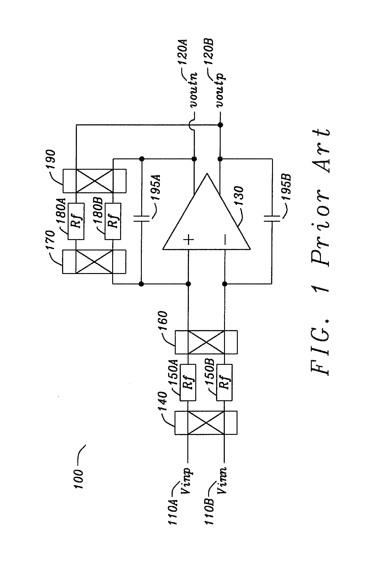
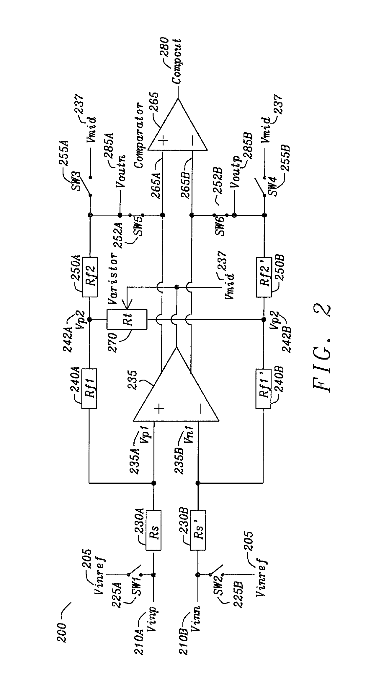
[0030]FIG. 2 is an amplifier circuit in accordance with the disclosure. The purpose of the invention is to achieve a high input common mode rejection (which could be in the order of 120 dB or greater) by matching the gain of both sides of a differential amplifier as depicted in FIG. 2. FIG. 2 show a first realization of the amplifier and its gain trimming circuit, depicted with the switches in normal operation mode.FIG. 2 is an embodiment of the circuit 200 where the correction is performed by trimming the feedback path. FIG. 1 is an amplifier with gain trim network where the differential low offset amplifier is used as a comparator, and a simple comparator is then used to convert its output to a digital bit for gain trimming. The current switch positions are normal amplifier operation. If all switches are toggled, the circuit is in gain trim mode.

[0031]The inputs of the differential amplifier are Vinp 210A and Vinn 210B. To perform gain trimming the switches SW1225A and SW2225B are...

second embodiment

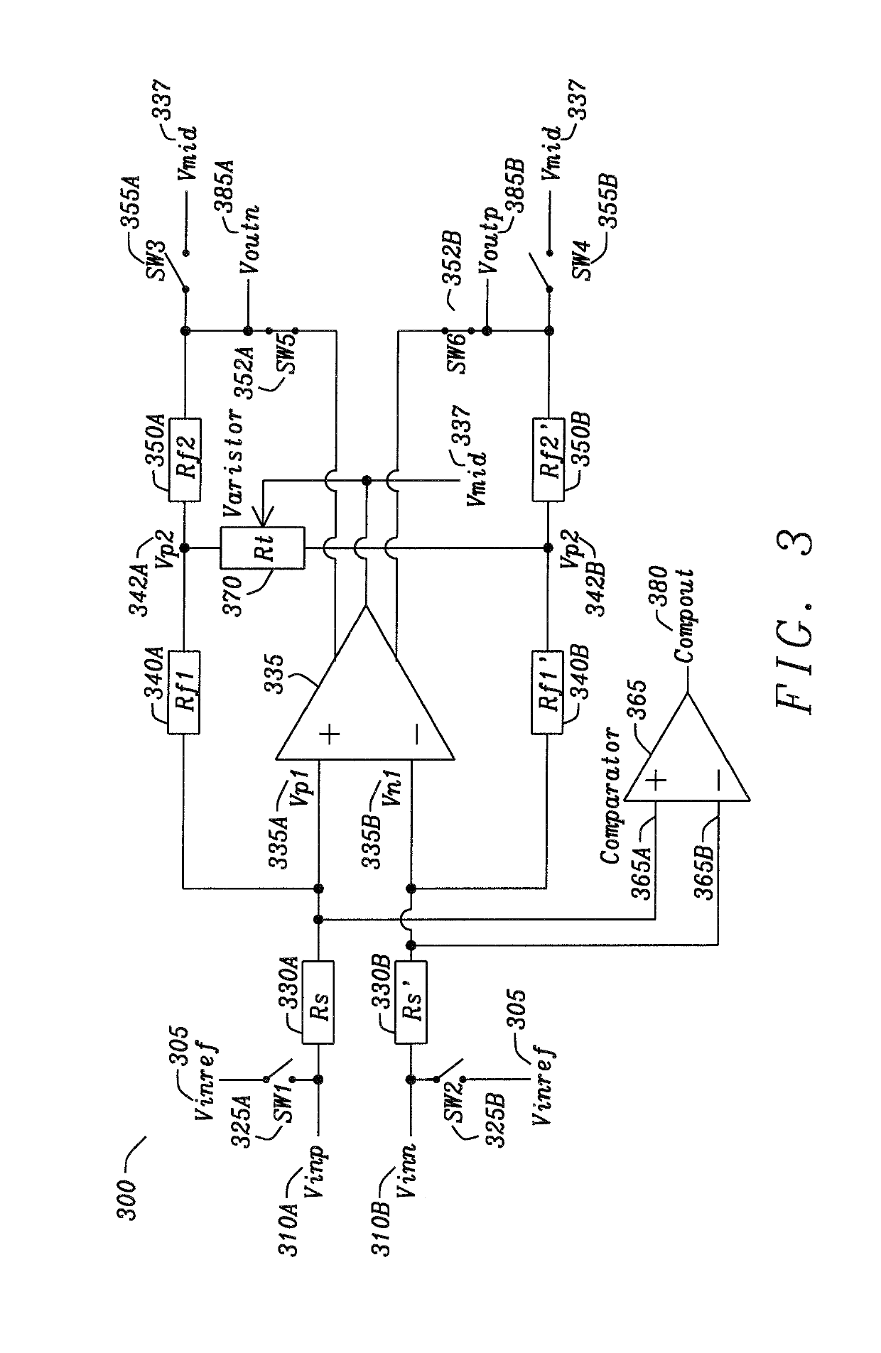
[0037]FIG. 3 is an amplifier circuit in accordance with the disclosure. FIG. 3 show a second realization of the amplifier and its gain trimming circuit, depicted with the switches in normal operation mode. FIG. 3 is an embodiment of the circuit where the correction is performed by trimming the feedback path. FIG. 3 is an amplifier with gain trim network separately where the differential amplifier is not used in the trim process. Current switch positions are normal amplifier operation. If all switches are toggled the circuit is in gain trim mode. The circuit 300 has inputs of the differential amplifier 335 are Vinp 310A and Vinn 310B. To perform gain trimming the switches SW1325A and SW2325B are toggled, causing following: (a) the inputs of the differential amplifier gain network to be tied to Vinref 305. The inputs have a series resistor Rs 330A and Rs' 330B. The differential amplifier 335 have input signals Vp1335A and Vn 335B. (b) the outputs of the differential amplifier gain net...

third embodiment

[0038]FIG. 4 is an amplifier circuit in accordance with the disclosure. FIG. 4 shows a circuit 400 where the trim is performed in the input resistance path. FIG. 2 is an alternative circuit realisation, where gain trim is performed by a T-network in the input resistors to the amplifier. Current switch positions are normal amplifier operation. If all switches are toggled the circuit is in gain trim mode. To perform gain trimming the switches SW1425A and SW2425B are toggled, causing following: (a) the inputs of the differential amplifier gain network to be tied to Vinref 405. The inputs have a series resistor Rs1430A and Rs1′430B; these are followed by Rs2432A and Rs2′432B. The differential amplifier 435 have input signals Vp1435A and Vn 435B. (b) the outputs of the differential amplifier network 435 are be tied to switch SW5452A and switch SW6452B. A feedback resistor Rf 440A is coupled to Vp1435A and a second feedback resistor Rf′435B is coupled to signal Vn1435B. The resistor Rf 44...


PUM


Abstract

An amplifier comprising a differential amplifier configured to be provide a comparator function, and a gain trimming circuit is electrically configured to provide gain trimming using a T-network comprising a varistor element. In addition, a method of trimming the gain of a differential amplifier, comprising the steps of a first step, (a) providing the differential amplifier comprising resistors in both of its paths, a second step, (b) providing a varistor in a T-network between both said paths; and lastly, a third step, (c) trimming the gain of the differential amplifier by adjusting the varistor's resistance.

Description

BACKGROUNDField[0001]The disclosure relates generally to a differential amplifier and, more particularly, to a gain trim circuit and method for trimming the amplifier's gain.Description of the Related Art[0002]One of the main methods of achieving a high input common mode rejection ratio (CMRR) in differential amplifiers is to use a chopper circuit to cancel out gain and offset caused by mismatches in the amplifier gain network. The input stage of the amplifier can also be chopped to minimise offset.[0003]FIG. 1 illustrates an example of a prior art amplifier known to the inventor. The differential amplifier 100 has two inputs Vinp 110A and Vinn 110B and output Voutn 120A and Voutp 120B of amplifier 130. In series with the input signals are chopper 140, series resistors 150A and 150B, and a second chopper 160. In the network, feedback resistor 180A and 180B, chopper 170 and 190, and capacitors 195A and 195B exist between the output signals and the input signals. The input stage of th...

Claims


Application Information

Patent Timeline
Patent Type & Authority Patents(United States)
IPC IPC(8): H03F3/45H03G1/00H03F3/387
CPCH03G1/0088H03F3/387H03F3/45475H03F3/45928H03F3/45977H03F2200/381H03F2203/45591H03F2203/45044H03F2203/45074H03F2203/45206H03F2203/45528H03F2203/45534H03F2203/45042
Inventor MENGAD, ZAKARIACOLLINS, STEVENVASILEV, VLADISLAV
Owner DIALOG SEMICON UK
Why Eureka
Try Eureka