
Energy-efficient power and offset allocation of spatial multiplexing in multimode fiber

a multi-mode fiber and energy-efficient technology, applied in multiplex communication, power management, data switching networks, etc., can solve the problems of inefficient copper-based interconnect technology, increased power consumption of data centers, and significant challenges in fiber volume, so as to maximize capacity

Active Publication Date: 2019-03-19
B G NEGEV TECH & APPL LTD
View PDF7 Cites 15 Cited by
  • Summary
  • Abstract
  • Description
  • Claims
  • Application Information

AI Technical Summary

Benefits of technology

The patent describes a technology that minimizes the electrical power consumed by optical transmitters in a network. The technology uses a modulation scheme to efficiently allocate power among multiple transmitters. The goal is to maximize the capacity of the network and improve its overall performance.

Problems solved by technology

On the other hand, this also means that the power consumed by data centers continues to grow exponentially and the fiber volume becomes a significant challenge.
Especially, as copper-based interconnect technology is inefficient, expensive and slow, the transition to optical interconnects has become a reality, with most of the power being consumed by sending data via interconnects within and between racks of servers.
502-506, March 2011), However, and to the best of the authors' knowledge, these previous works did not look into analytical approaches to optimally allocate system parameters, such as electrical power, and DC offset of the modulated signal.

Method used


Image

  • Energy-efficient power and offset allocation of spatial multiplexing in multimode fiber
  • Energy-efficient power and offset allocation of spatial multiplexing in multimode fiber
  • Energy-efficient power and offset allocation of spatial multiplexing in multimode fiber

Examples


Embodiment Construction

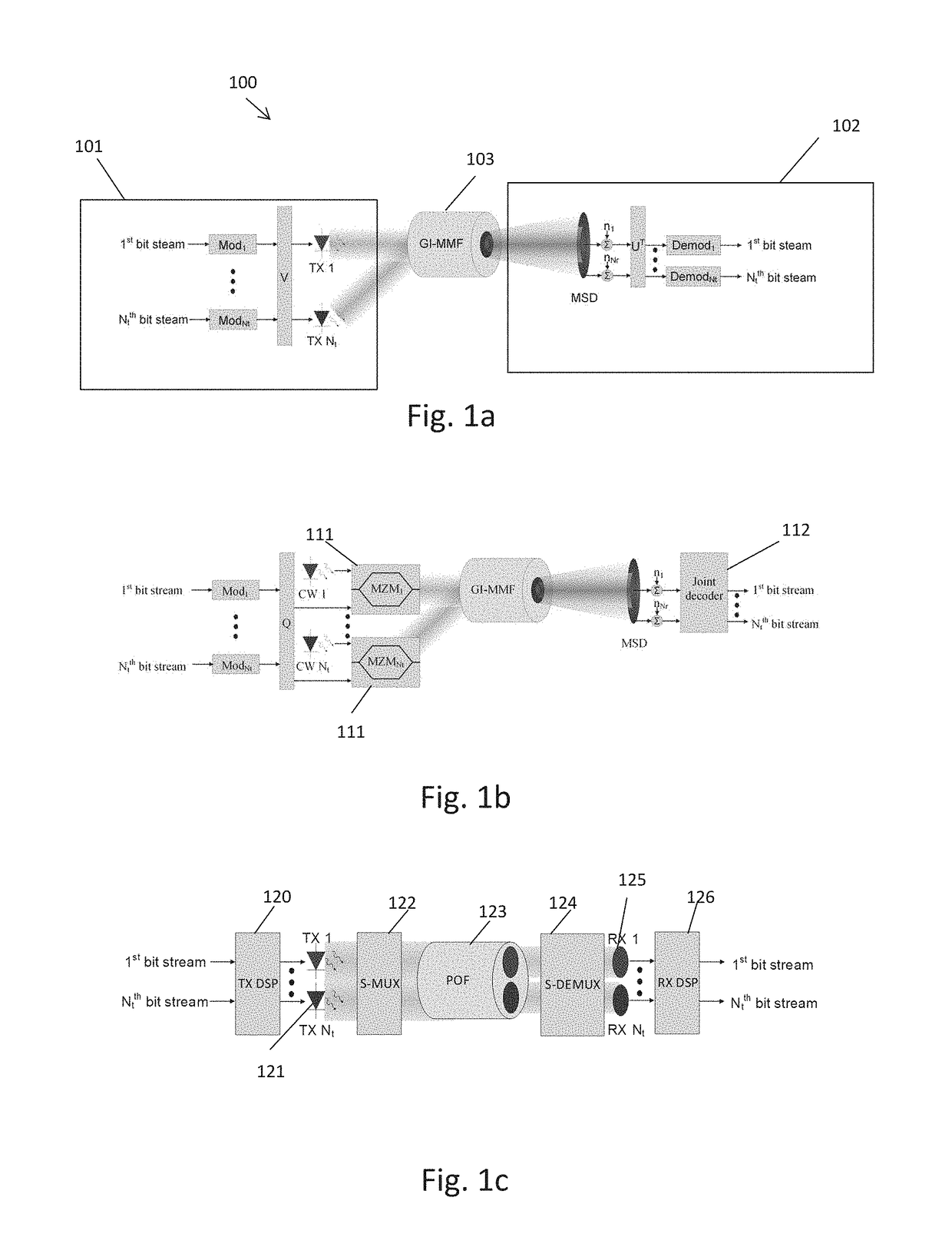
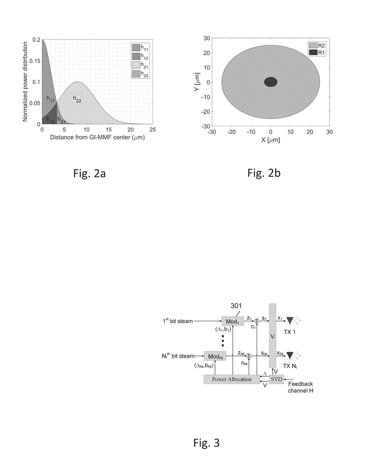
[0058]The present invention relates to a system and method for optimizing power allocation for each optical transmitter in an optical transmission system which is consisted of at least two intensity modulated optical transmitters, an optical channel that can be spatially multiplexed and at least two direct detection optical detectors. The power allocation minimizes the electrical power consumption of the optical transmitters, by using energy efficient convex optimization to a mode-group-division-multiplexing, multiple-input-multiple-output (MIMO) scheme, which includes for example: a Vertical Cavity Surface Emitting Lasers (VCSEL) array with multi-segment concentric photo-detector.

[0059]The system of the present invention MIMO output architecture may be based upon (but not limited to), Singular Value Decomposition (SVD). Alternatively the present invention MIMO output architecture may be based upon (but not limited to), Vertical Bell Labs Layered Architecture Space Time (V-BLAST).

[0...


PUM


Abstract

A system for optimizing power allocation for each optical transmitter in an optical transmission system, the system comprises at least two intensity modulated optical transmitters, each of which is controlled by a modulator; an optical channel that can be spatially multiplexed by a multiplexer; and at least two optical detectors, for detecting the transmitted modulated signals. Each of the modulators are adapted to modulate the transmitters such that the electrical power consumption of the optical transmitters is minimized by a modulation scheme of the modulators, that uses energy efficient convex optimization to multiplex the transmitted optical signals, by the multiplexer in a multiple-input-multiple-output (MIMO) scheme. Each of the modulators are adapted to modulate the transmitters such that the capacity is maximized by a modulation scheme of the modulators, that uses energy efficient convex optimization to multiplex the transmitted optical signals, by the multiplexer in a multiple-input-multiple-output (MIMO) scheme.

Description

FIELD OF THE INVENTION[0001]The invention is in the field of optical transmission systems. More specifically the invention relates to energy efficient power and offset allocation of spatial multiplexing in multimode fiber.BACKGROUND OF INVENTION[0002]In recent years, an exponential data traffic and electrical power consumption growth is exhibited in high performance computing (HPC) interconnects. Thus, Green Photonics, which tries to minimize the Joule / bit ratio becomes a major subject of both public and scientific interest. A significant amount of the installations within these HPCs are graded-index multimode fibers (GI-MMFs) using parallel rack-to-rack optical interconnects. These fibers enable the use of mode division multiplexing to increase the fiber's capacity.[0003]High speed transmission systems (>10 Gb / s) for short-reach interconnects, such as data-centers and high performance computing (HPC), attracts extensive interest due to the exponential data traffic growth in such...

Claims


Application Information

Patent Timeline
IPC IPC(8): H04B7/06H04L12/24H04W52/34H04J14/02H04B7/0426H04W52/42
CPCH04B7/0426H04J14/0241H04L41/0826H04W52/346H04B7/0602H04W52/42H04B7/0697H04B10/2581H04J14/04
Inventor SADOT, DANSHEFFI, NIR
Owner B G NEGEV TECH & APPL LTD
Learn More