Optoelectronic device and smart window comprising the same

a technology of optoelectronic devices and smart windows, applied in door/window protective devices, instruments, constructions, etc., can solve the problems of high hvac cost, difficult to create durable, low-power windows that can induce large, reversible changes using applied voltage, and difficult to create durable, low-power windows. , to achieve the effect of reducing the operating range of applied voltage, reducing the cost of operation, and improving the quality of operation

Active Publication Date: 2019-01-29
SAMSUNG ELECTRONICS CO LTD +1
View PDF11 Cites 0 Cited by
  • Summary
  • Abstract
  • Description
  • Claims
  • Application Information

AI Technical Summary

Benefits of technology

[0008]To overcome the previously mentioned obstacles, an ionic liquid (IL) gating technique is used in certain embodiments to dynamically tune the optical properties in layered structure materials. According to certain embodiments, the general architecture is similar to a metal-on-semiconductor field effect transistor (MOSFET); a source and drain electrode are in contact with the active material and a gate electrode is placed away from the rest of the device. Then, an ionic liquid, e.g., an ionic salt that is liquid at room temperature, is applied over the device and takes the place of where the oxide dielectric would be in a MOSFET. By changing the voltage at the gate, large electron concentrations are induced, which ultimately change the optical properties of the active material. This novel IL technique demonstrated a tunable transmission window in ultrathin nanoplates (on the order of a few nanometers to tens of nanometers thick) in the visible and near infrared regions, with a low applied voltage operation range, e.g., from −3V˜3V, which is equivalent to a typical AA battery. This allows for various embodiments to be used in any application that requires electrical control of the reflection, transmission, and absorption properties of a material.
[0009]Compared to using oxide dielectrics, the EDL techniques of the present embodiments offer lower-power, and a much stronger carrier concentration tuning ability. This leads to a greater change in transparency with a lower power consumption. The EDL gating approach of the present embodiments not only provides a powerful method for modulating the electronic transport and other physical properties in materials such as Bi2Se3, but also simplifies device fabrication. The EDL can be applied using a pipette to apply a small drop. Ionic liquids are prone to breakdown failure outside their electrochemical window, the largest voltage that can be applied before failure, which causes irreversible damage. Fortunately, changes up to 50% are possible well before the failure voltage.
[0010]Electrochromicity is another popular method of inducing similar changes in an active material. Electrochromicity has the advantage of being an established technology and the current standard for smart windows. It also does not require a constant applied voltage to keep a particular opacity level. Electrochromicity, however, uses chemical reactions in order to induce changes which can cause instability and unwanted byproducts. The embodiments herein depend on promoting charge carriers and are much more stable. Electrochromics are also prone to overheating. Ionic liquids are stable at high temperatures, decreasing the chance of failure from increased absorption. The present embodiments are also more powerful than electrochromics, inducing much larger changes over the same voltage range. This also allows thinner active layers to be used, reducing material consumption, fabrication costs and time.

Problems solved by technology

Altering the transmission of materials in the visible spectrum remains a formidable challenge, due to the difficulties of tuning the Fermi Level and charge-carrier density over a wide range.
This is primarily caused by high heating, ventilation, and air conditioning (HVAC) costs.
However, it is difficult to create durable, low power windows that can induce large, reversible changes using an applied voltage.
The best performing windows are also quite costly.
Ionic liquids are prone to breakdown failure outside their electrochemical window, the largest voltage that can be applied before failure, which causes irreversible damage.
Electrochromicity, however, uses chemical reactions in order to induce changes which can cause instability and unwanted byproducts.
Electrochromics are also prone to overheating.
Other methods, such as thermochromicity and liquid crystals, are either unable to be controlled electrically or require much higher voltages and power to induce the changes.

Method used


Image

  • Optoelectronic device and smart window comprising the same
  • Optoelectronic device and smart window comprising the same
  • Optoelectronic device and smart window comprising the same

Examples


Embodiment Construction

[0053]Reference will now be made in detail to exemplary embodiments, examples of which are illustrated in the accompanying drawings, wherein like reference numerals refer to like elements throughout. In this regard, the present exemplary embodiments may have different forms and should not be construed as being limited to the descriptions set forth herein. Accordingly, the exemplary embodiments are merely described below, by referring to the FIG.s, to explain aspects thereof. Expressions such as “at least one of,” when preceding a list of elements, modify the entire list of elements and do not modify the individual elements of the list. An expression used in the singular may encompass the expression in the plural.

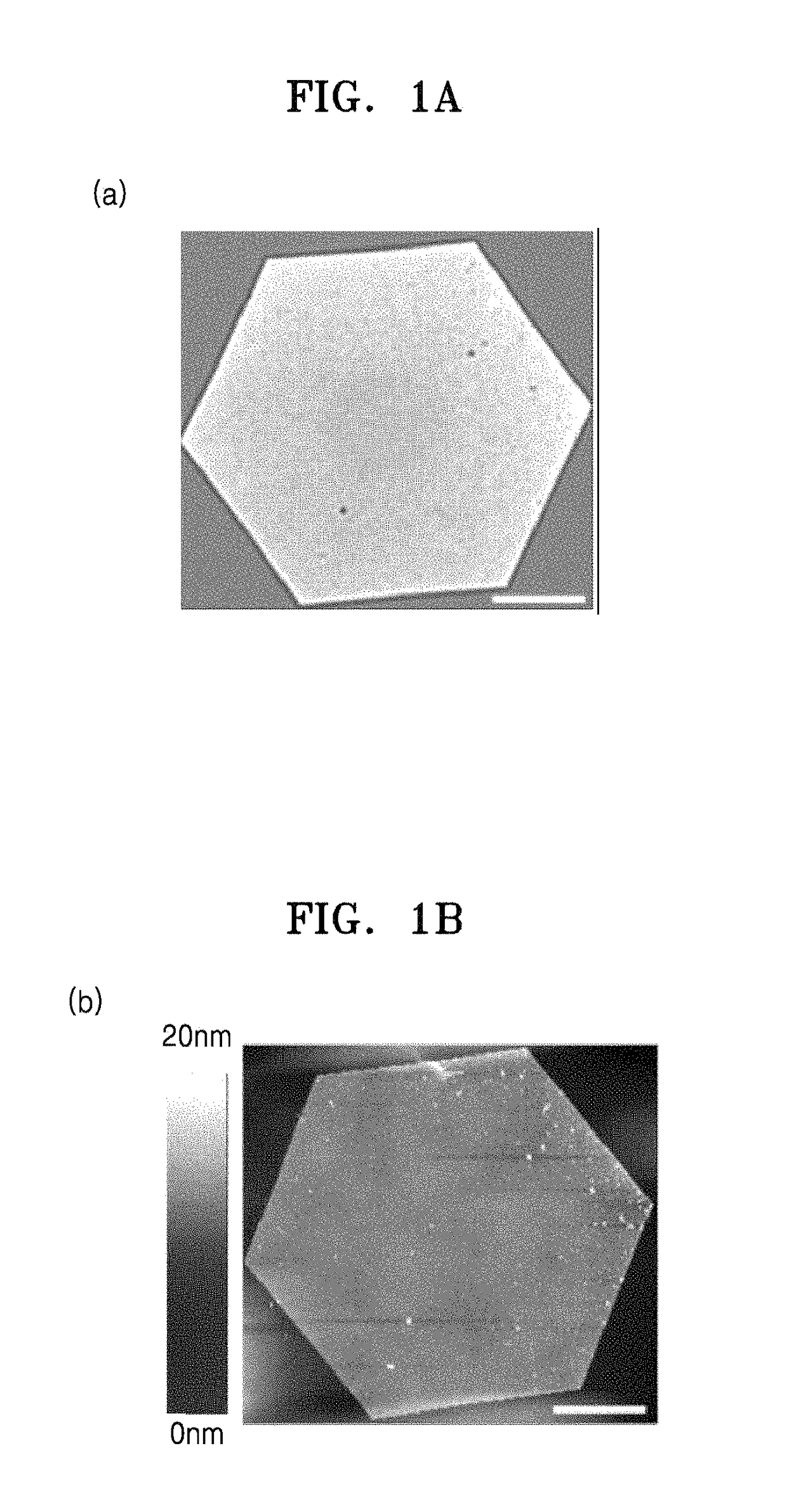
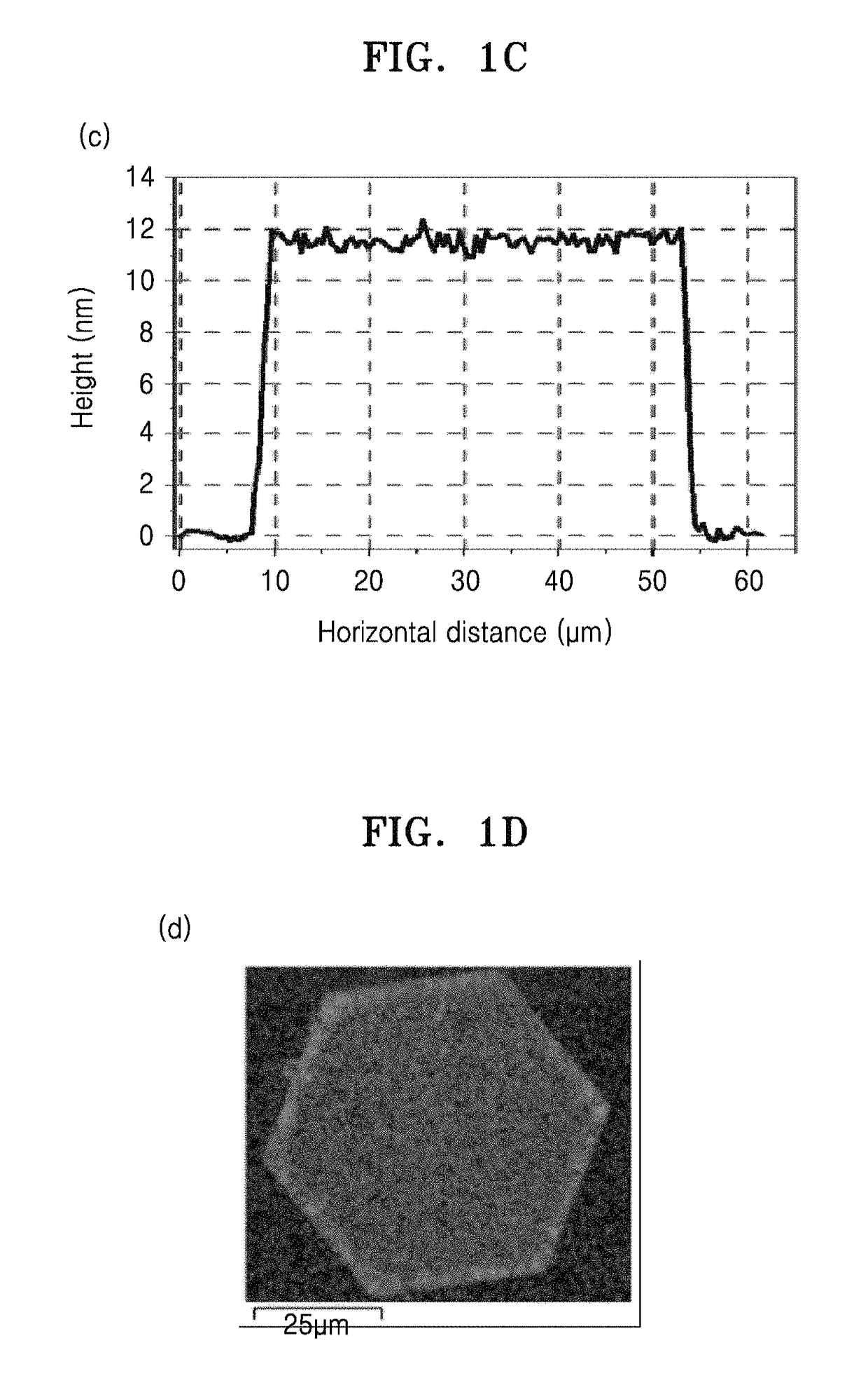
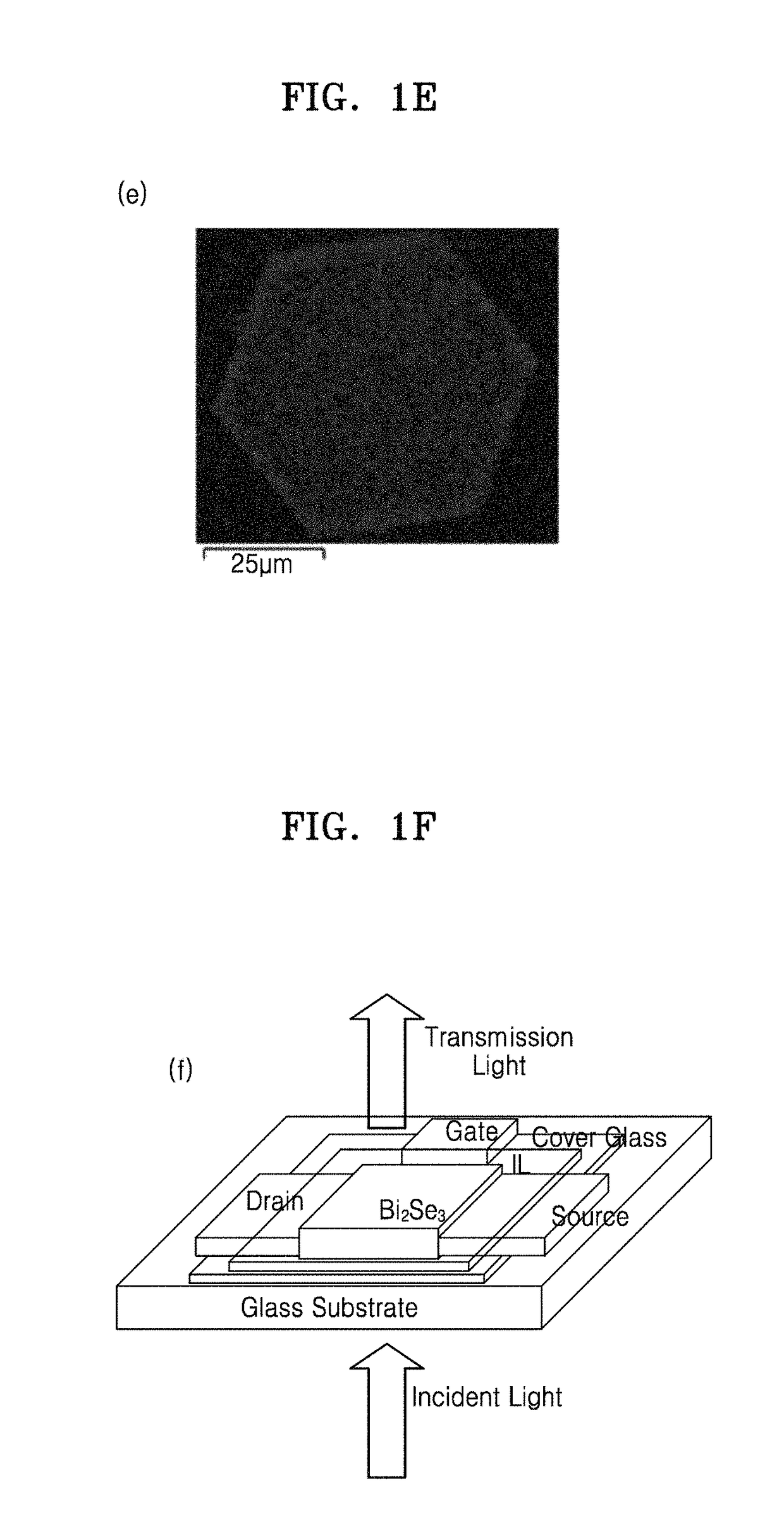
[0054]A detailed description of an optical modulator including a nanostructure will be presented below with reference to the drawings. A size of each component in the drawings may be exaggerated for the sake of convenience. In addition, the exemplary embodiments described be...


PUM

PropertyMeasurementUnit
thicknessaaaaaaaaaa
thicknessaaaaaaaaaa
thicknessaaaaaaaaaa

Abstract

Provided is an optical modulator having high resolution and being capable of controlling a wavelength range of reflected / transmitted light. The optical modulator may include a plurality of nanostructures capable of changing refractive index and a first insulation layer surrounding the plurality of nanostructures. The refractive index of each of the nanostructures may be greater than that of the first insulation layer. The nanostructures may modulate light depending on a change in the refractive index thereof. A change in a resonance wavelength, intensity, phase, polarization, etc. of reflected / transmitted light may be generated.

Description

CROSS-REFERENCE TO RELATED APPLICATIONS[0001]This application claims the benefit of U.S. Provisional Application No. 62 / 265,816, filed on Dec. 10, 2015, in the US Patent Office and Korean Patent Application No. 10-2016-00166884, filed on Dec. 8, 2016, in the Korean Intellectual Property Office, the disclosures of which are incorporated herein in their entireties by reference.BACKGROUND[0002]1. Field[0003]The present disclosure generally provides optoelectronic devices incorporating layered structured materials and semiconductor thin films, and more particularly to control of the optical properties of such materials.[0004]2. Description of the Related Art[0005]Reducing energy consumption has become one of the primary goals for the world due to the onset of global warming and the potential for reducing costs for device operation. It is therefore favorable to find low power device alternatives to current technology, or devices that can indirectly reduce power consumption. This is espec...

Claims


Application Information

Patent Timeline
Patent Type & Authority Patents(United States)
IPC IPC(8): G02F1/061G02B1/14E06B7/28E06B9/24G02B26/02
CPCG02F1/061E06B7/28E06B9/24G02B1/14G02B26/02G02F2202/36E06B2009/2464G02F2201/12G02F2202/02
Inventor HAN, SEUNGHOONLIU, YANPINGYAO, JIETOM, KYLE
Owner SAMSUNG ELECTRONICS CO LTD
Why Eureka
Try Eureka