Method for producing a data carrier that prevents mechanical strains between chip and data carrier body

a data carrier and mechanical strain technology, applied in the field of data carrier manufacturing, can solve the problems of affecting the performance the durability of the data carrier, and the lack of dedicated user data output,

Active Publication Date: 2019-01-08
GIESECKE & DEVRIENT MOBILE SECURITY GMBH
View PDF26 Cites 0 Cited by
  • Summary
  • Abstract
  • Description
  • Claims
  • Application Information

AI Technical Summary

Benefits of technology

The invention is a stabilizing agent that helps to integrate a chip with a data carrier body during a lamination process. The stabilizing agent is applied before the lamination and remains flexible during the process, avoiding mechanical tension between the chip and the carrier body. The stabilizing agent can be activated by UV or hot-melt radiation and can be applied using a metering unit or printing technology. The technical effects of this invention are that it simplifies the manufacturing process, accelerates it, and ensures accurate and quantitative application of the stabilizing agent.

Problems solved by technology

It frequently possesses no, or only a rudimentary, dedicated user data output.
A problem with respect to the durability of such data carriers is the bond between the chip and the data carrier body.
A cause for the formation of cracks can be found in the mechanical load on the data carriers, by means of which the mechanical tensions frozen in the data carrier body are released.
In particular, a formation of cracks or, likewise, a breaking of a layer of the data carrier body, for example of a foil layer occurs.
These cracks may propagate into the nearest foil layer.
In particular the electrical functionality, the appearance, the ruggedness against external environmental influences and also the mechanical stability of the data carrier are impaired by the cracks.
In extreme cases, the electrical functionality of the data carrier, in particular the contactless reading of / bringing data from / into the IC of the data carrier is no longer possible.
The realization of the patchwork-like layers is elaborate, however, and, moreover, the plastic material is difficult to position.
The problem in all of these propositions is that the mechanical tensions between chip, electronic components and data carrier body, which were introduced during the lamination, cannot be sufficiently compensated, because adhesive and chip form a mechanical unit already before the lamination.
This leads to mechanical tensions in the data carrier during the lamination.
Upon proper use of the data carrier, these tensions lead to the described formation of cracks.

Method used


Image

  • Method for producing a data carrier that prevents mechanical strains between chip and data carrier body
  • Method for producing a data carrier that prevents mechanical strains between chip and data carrier body
  • Method for producing a data carrier that prevents mechanical strains between chip and data carrier body

Examples


Embodiment Construction

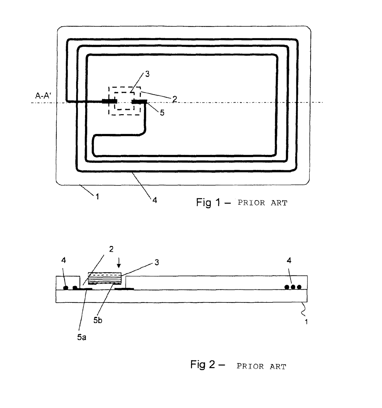
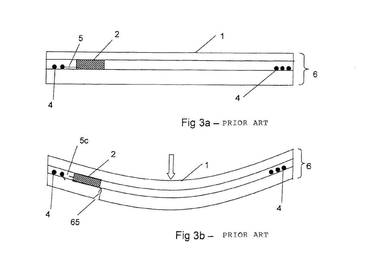
[0046]FIG. 1 shows a data carrier 1 in plan view with an incorporated near-field antenna according to the today's prior art. A gap 2 is incorporated in the data carrier body 6. This gap 2 can be manufactured in different ways, for example by constructing the data carrier body 6 in layers with a corresponding gap 2 in one of the layers. Into the gap 2 there is incorporated a chip 3. The chip 3 either is an integrated semiconductor chip arranged with contact pads on a substrate, which semiconductor chip is incorporated into the data carrier body 6 such that a contacting of the chip by means of an external end device is possible. Alternatively, the chip is a molded semiconductor chip, which is incorporated into the gap 2 to be electroconductively connected with contacting points 5 of the data carrier body 6 there. The contacting points 5 in turn are connected with a near-field antenna 4, in the following referred to as coil 4, arranged in the data carrier body 6.

[0047]Such data carrier...


PUM

PropertyMeasurementUnit
electroconductiveaaaaaaaaaa
flexibleaaaaaaaaaa
sizeaaaaaaaaaa

Abstract

This disclosure includes a method for manufacturing a portable data carrier, an inlay for a data carrier, and a data carrier. A data carrier body has a gap for a chip and a chip is incorporated into the gap. In a subsequent step a cover layer is laid on the data carrier body, and the data carrier body and the cover layer are laminated. After the incorporation of the chip and before the lamination, a stabilizing agent is applied into the gap of the core layer, which remains soft or flexible during the lamination and cures or is activated (e.g. by means of UV radiation) only after the lamination, in order for mechanical tensions to be avoided.

Description

BACKGROUND[0001]The invention relates to a method for manufacturing a data carrier, an inlay for a data carrier, as well as to a data carrier itself. The invention relates in particular to a method for manufacturing a contactlessly readable data carrier with integrated IC, which can be used as a chip card, identification document, identity card or as a data page in a passport booklet.[0002]A portable data carrier is basically a computer with a reduced overall size and resource range, which has a microcontroller and at least one interface for communication with an external device. It frequently possesses no, or only a rudimentary, dedicated user data output. Its outer construction form is so designed that it can be easily carried by a user at any time. Preferably, a data carrier is equipped with corresponding security functionalities, for example in the form of a smart card, chip card, mass memory card, multimedia card. For example a payment card, such as credit or debit cards, is a ...

Claims


Application Information

Patent Timeline
Patent Type & Authority Patents(United States)
IPC IPC(8): G06K19/077
CPCG06K19/07728G06K19/07749G06K19/07722Y10T29/49018
Inventor PONIKWAR, WALTERTARANTINO, THOMASSALZER, TOBIASBRAUN, ANDREASENDRES, GUNTER
Owner GIESECKE & DEVRIENT MOBILE SECURITY GMBH
Why Eureka
Try Eureka