Irregular shape display device having hole
a display device and irregular shape technology, applied in the field of irregular shape display devices, can solve the problems of more restrictive structure, more restrictive molding and dimensional design errors, etc., and achieve the effects of reducing luminance differences, improving dark portions, and enhancing image quality
- Summary
- Abstract
- Description
- Claims
- Application Information
AI Technical Summary
Benefits of technology
Problems solved by technology
Method used
Image
Examples
first embodiment
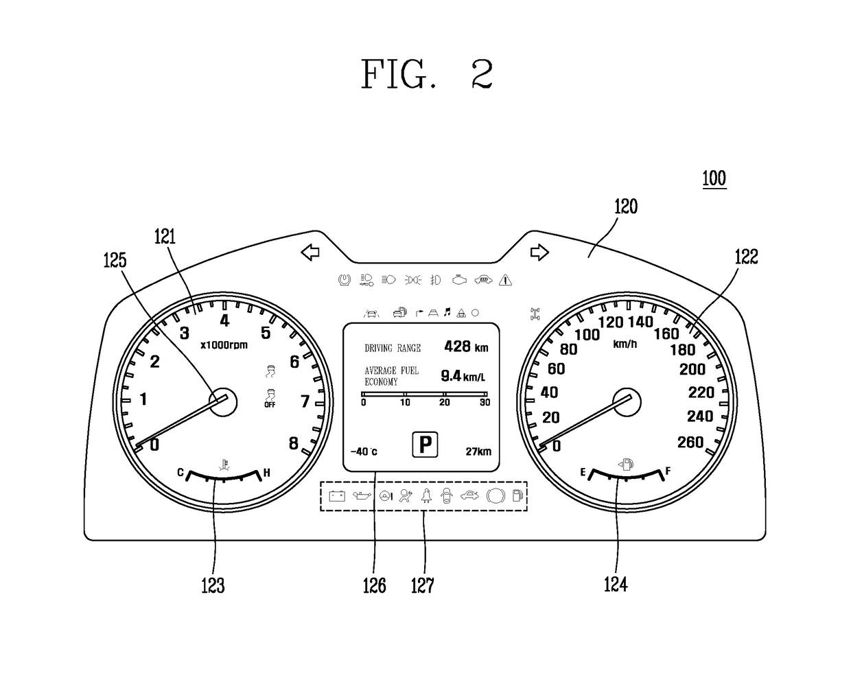
[0066]FIG. 2 is a plan view illustrating an irregular shape display according to the present disclosure for an example.
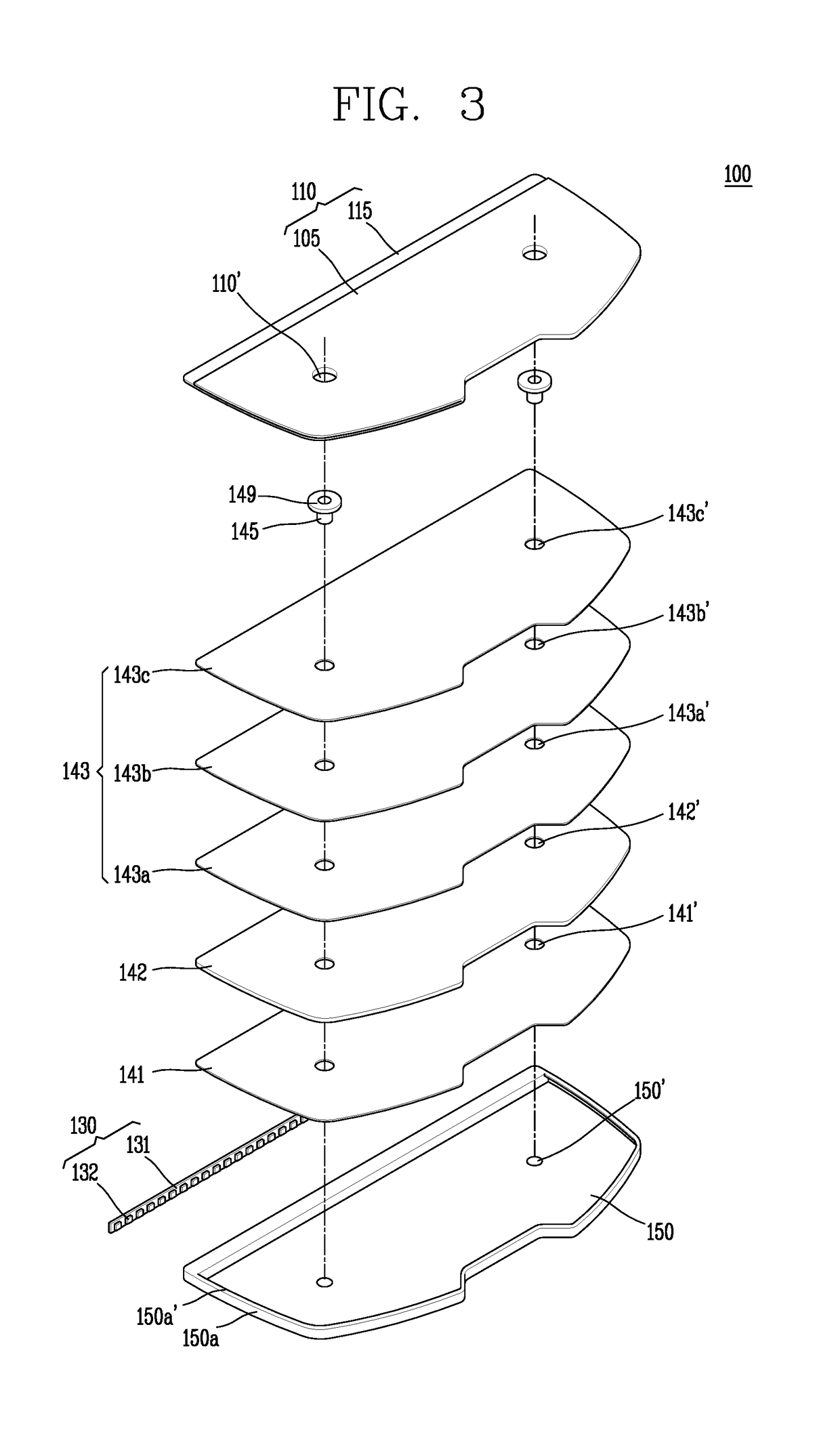
[0067]FIG. 3 is an exploded perspective view schematically illustrating the structure of the irregular shape display according to the first embodiment of the present disclosure illustrated in FIG. 2.
[0068]FIG. 4 is a view schematically illustrating the planar structure of a low cover in the irregular shape display according to the first embodiment of the present disclosure illustrated in FIG. 2.
[0069]FIG. 5 is a view schematically illustrating a cross-section taken along line A-A′ in the irregular shape display according to the first embodiment of the present disclosure illustrated in FIG. 4, and FIG. 6 is a view schematically illustrating a cross-section taken along line B-B′ in the irregular shape display according to the first embodiment of the present disclosure illustrated in FIG. 4. In other words, FIG. 5 illustrates a cross-section around a hole as an example...
second embodiment
[0147]FIG. 9 is a view schematically illustrating a partial cross-section of an irregular shape display according to the present disclosure.
[0148]Furthermore, FIG. 10 is a view schematically illustrating another partial cross-section of the irregular shape display according to the second embodiment of the present disclosure.
[0149]Here, FIG. 9 illustrates a cross-section around the hole as an example, and FIG. 10 illustrates a cross-section of an edge portion of the hole as an example.
[0150]Furthermore, the irregular shape display according to the second embodiment of the present disclosure illustrated in FIGS. 9 and 10 may have substantially the same configuration as that of the foregoing first embodiment of the present disclosure except for the liquid crystal panel being mounted on the reflection sheet.
[0151]Referring to FIGS. 9 and 10, the irregular shape display according to the second embodiment of the present disclosure may include a liquid crystal panel 210 in which liquid cry...
third embodiment
[0160]The reflector 241 is located between the lower cover 250 and a rear surface of the light guide plate 242. The reflector 241 performs the role of reflecting light from the light source and light from the light guide plate 242 to the side of the liquid crystal panel 210. Here, FIGS. 11 and 12 illustrate a case where a reflector 341 is formed in a shape of surrounding an edge side of a light guide plate 342 as an example, which will be explained more fully as a
[0161]Furthermore, the light source may be selected from any one of CCFL, HCFL, EEFL and LED, but may not be necessarily limited to this. Hereinafter, for the sake of convenience of explanation, a case where an LED array is used for the light source will be taken as an example.
[0162]The LED array is provided on a flexible printed circuit board such that a light exit surface thereof faces an incident surface of the light guide plate 242. In other words, the light source unit may include the flexible printed circuit board and...
PUM
| Property | Measurement | Unit |
|---|---|---|
| thickness | aaaaa | aaaaa |
| size | aaaaa | aaaaa |
| size | aaaaa | aaaaa |
Abstract
Description
Claims
Application Information
 - R&D
- Intellectual Property
- Life Sciences
- Materials
- Tech Scout
- Unparalleled Data Quality
- Higher Quality Content
- 60% Fewer Hallucinations
Browse by: Latest US Patents, China's latest patents, Technical Efficacy Thesaurus, Application Domain, Technology Topic, Popular Technical Reports.
© 2025 PatSnap. All rights reserved.Legal|Privacy policy|Modern Slavery Act Transparency Statement|Sitemap|About US| Contact US: help@patsnap.com


