Electronic device and method for manufacturing electronic device

a manufacturing method and electronic device technology, applied in the manufacture of final products, printed circuit non-printed electric components, electric apparatus casings/cabinets/drawers, etc., can solve the problems of deterioration of electronic parts and energy loss, increase in esr, complicated manufacturing process, etc., to achieve easy manufacturing of electronic devices, easy to manufacture, and uniform application of conductive bonding agents

Active Publication Date: 2018-07-24
MURATA MFG CO LTD
View PDF5 Cites 1 Cited by
  • Summary
  • Abstract
  • Description
  • Claims
  • Application Information

AI Technical Summary

Benefits of technology

[0015]The present invention has been made in light of such a condition, and an object of the present invention is to provide a reliable electronic device in which an ESR is low and which has a fuse function with good fusing characteristics, and an electronic device manufacturing method which can efficiently manufacture this electronic device at low cost.
[0039]Since the flexible substrate and the rigid substrate are separately made, and are bonded with the conductive bonding agent interposed therebetween, it is not necessary to make the intermediate connection layer by using an expensive rigid flexible substrate of an integrated structure. Consequently, it is possible to easily manufacture the electronic device in which an ESR is reduced and which has a desired fuse function at low cost. Further, the flexible substrate and the rigid substrate are bonded by the conductive bonding agent, so that it is not necessary to adhere the rigid substrate and the flexible substrate by an adhesive for temporal adhesion, either, and it is possible to simplify the manufacturing process. Furthermore, the conductive bonding agent is applied to the rigid substrate to secure electrical conduction in the intermediate connection layer via the conductive bonding agent, so that it is not necessary to perform via processing for making conduction vias and plate processing. Still further, even when heat loads are repeatedly applied at fixed cycles, it is possible to prevent occurrence of a disconnection failure.

Problems solved by technology

Further, an increase in the ESR increases a heat generation amount and causes deterioration of the electronic part and energy loss.
Furthermore, the rigid flexible substrate of the above integrated structure needs an adhering process to adhere the rigid portions 106a and 106b and the flexible portion 105, and therefore is expensive.
That is, according to International Publication No. 2016 / 039260, there is a concern that the ESR increases, the manufacturing process is complicated and manufacturing cost steeply rises.

Method used


Image

  • Electronic device and method for manufacturing electronic device
  • Electronic device and method for manufacturing electronic device
  • Electronic device and method for manufacturing electronic device

Examples


example

[0129]A multilayer ceramic capacitor was mounted on an intermediate connection layer to conduct a heat cycle test.

[0130][Making of Flexible Substrate]

[0131]A flexible mother board was prepared, which was 8.0 mm in length and was 6.2 mm in width, and was formed by adhering a copper foil which was 18 μm in thickness to both top and back surfaces of a polyimide resin which was 25 μm in thickness was prepared.

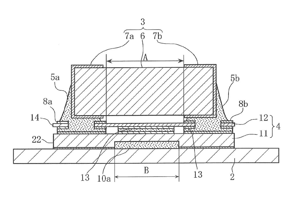
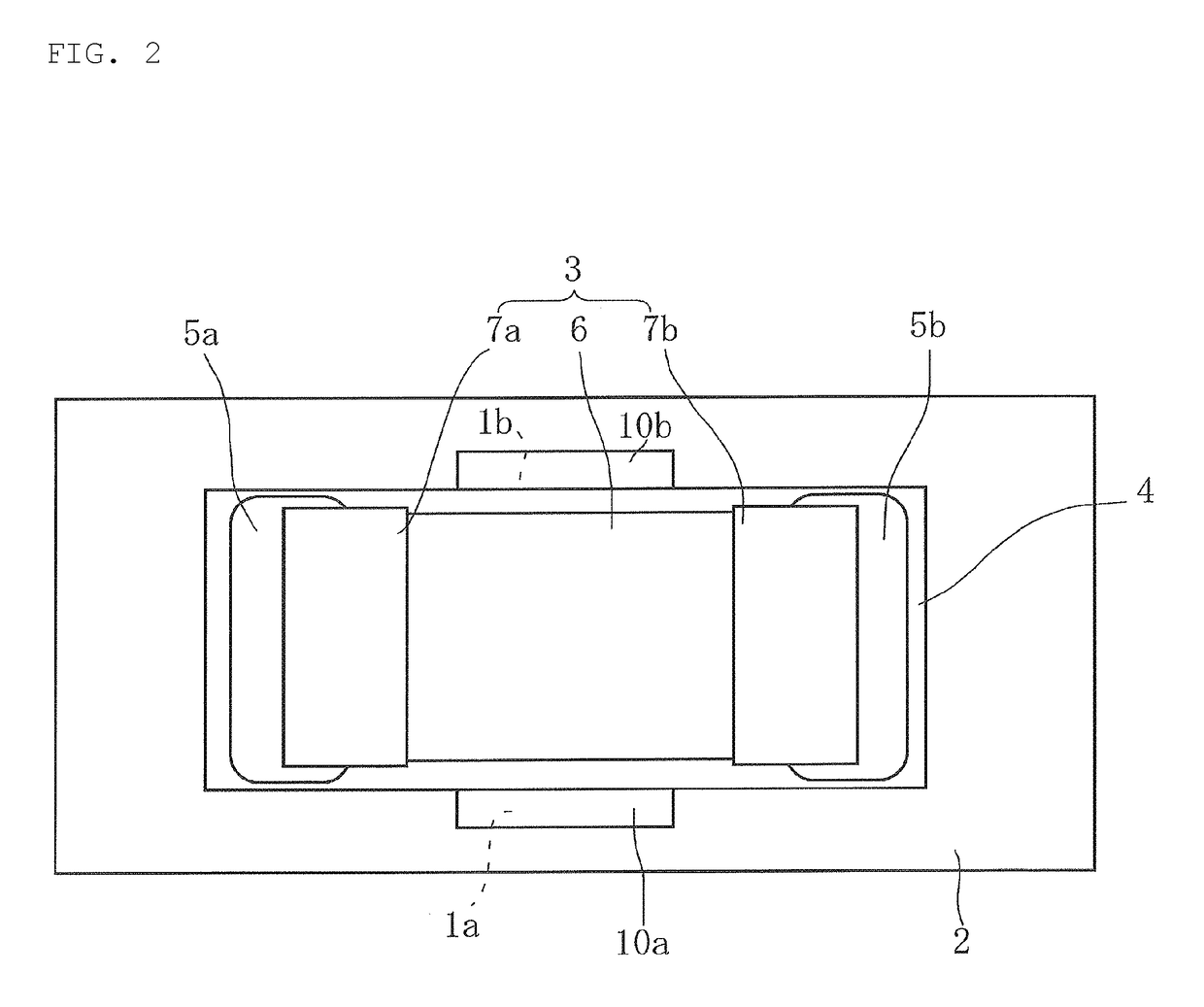
[0132]Next, a photolithography technique was applied to this flexible mother board to form first and second conductor portions which were 4.8 mm in height and were 2.1 mm in width at predetermined portions of a top surface of the flexible mother board. In this regard, the conductor portion interval A was 3.5 mm.

[0133]Similarly, a third conductor portion was made also at a back surface side of the flexible mother board, composed of a main conductor portion whose rectangular portion was 4.8 mm in height and 2.05 mm in width and whose portion continuing to this rectangular portion was...


PUM

PropertyMeasurementUnit
thicknessaaaaaaaaaa
thicknessaaaaaaaaaa
thicknessaaaaaaaaaa

Abstract

An intermediate connection layer interposed between a wiring substrate and an electronic part includes a rigid substrate and a flexible substrate. A plurality of conductor portions are formed on opposed principal surfaces of the respective flexible and rigid substrates. The rigid substrate is provided with an opening, and a fuse portion on the flexible substrate faces the opening. The flexible substrate and the rigid substrate are bonded together with solders. The respective rigid and flexible substrates are separately made, solder pastes are applied to the rigid substrate, both substrates are overlaid on each other, and the solder pastes are heated and solidified to make the intermediate connection layer.

Description

CROSS REFERENCE TO RELATED APPLICATIONS[0001]The present application claims priority to Japanese Patent Application No. 2016-114178, filed Jun. 8, 2016, the entire contents of which are incorporated herein by reference.BACKGROUND OF THE INVENTIONField of the Invention[0002]The present invention relates to an electronic device and an electronic device manufacturing method, and, more specifically, the present invention relates to an electronic device in which electronic parts such as a chip multilayer ceramic capacitor are mounted and an electronic device manufacturing method.Description of the Related Art[0003]Conventionally, a surface mounting technique of mounting electronic parts such as a chip multilayer ceramic capacitor on a substrate is widely known. Further, according to surface mounting techniques of this type, electronic devices in which an intermediate connection layer having a fuse function is interposed between an electronic part and a wiring substrate to prevent a mount...

Claims


Application Information

Patent Timeline
Patent Type & Authority Patents(United States)
IPC IPC(8): H05K5/00H05K3/34H05K3/36H05K3/40H05K3/12H05K3/00H05K1/03H01G4/30H05K1/18H05K7/00H05K1/14H05K1/11H05K1/02H05K3/46
CPCH05K1/189H05K1/028H05K1/0293H05K1/0393H05K1/115H05K1/144H05K1/181H05K3/0052H05K3/12H05K3/3442H05K3/3494H05K3/363H05K3/4038H01G4/30H05K2201/20H05K1/02H05K1/0298H05K1/11H05K1/118H05K1/147H05K1/148H05K3/4691H05K2201/049H05K2201/05H05K2201/10015H01G4/12H05K13/046H05K13/0465H01G2/06H01G4/232H01G4/40H05K2201/10181H05K2201/10515H05K2201/1053Y02P70/50H01H85/205H05K1/182H05K3/321
Inventor SAKAMOTO, HIROKI
Owner MURATA MFG CO LTD
Why Eureka
Try Eureka