
LED device having individually addressable LED modules

a technology of led modules and led modules, which is applied in semiconductor devices, light sources, lighting and heating apparatus, etc., can solve the problems of limiting the achievable density of the array, the light intensity of the device, and the significant disadvantage of substantially limiting the heat dissipation capacity of the devi

Active Publication Date: 2018-07-24
KONINKLJIJKE PHILIPS NV
View PDF7 Cites 0 Cited by
  • Summary
  • Abstract
  • Description
  • Claims
  • Application Information

AI Technical Summary

Benefits of technology

This configuration enables finer spacing between LED modules, improved heat dissipation, and increased LED array density, while maintaining flexibility in lighting modes and beam shaping capabilities.

Problems solved by technology

Wiring tracks running along (i.e. parallel and coincident with) spaces between array rows and / or columns, as utilised by state of the art devices to enable individual addressability, consume valuable space, thereby limiting the achievable density of the array, and hence the light intensity of the device.
However, multi-layer wiring solutions of this sort carry the significant disadvantage of substantially limiting heat dissipation capacity within the device.
One or more wiring layers running through the substrate layer impede this thermal path, significantly diminishing the thermal conductivity between the LEDs and the heat-sink.
Additionally such wiring layers also increase costs, since a multilayer-type substrate is required, and also risk compromising reliability, since vias are required for connecting to internal layers.

Method used


Image

  • LED device having individually addressable LED modules
  • LED device having individually addressable LED modules
  • LED device having individually addressable LED modules

Examples


Embodiment Construction

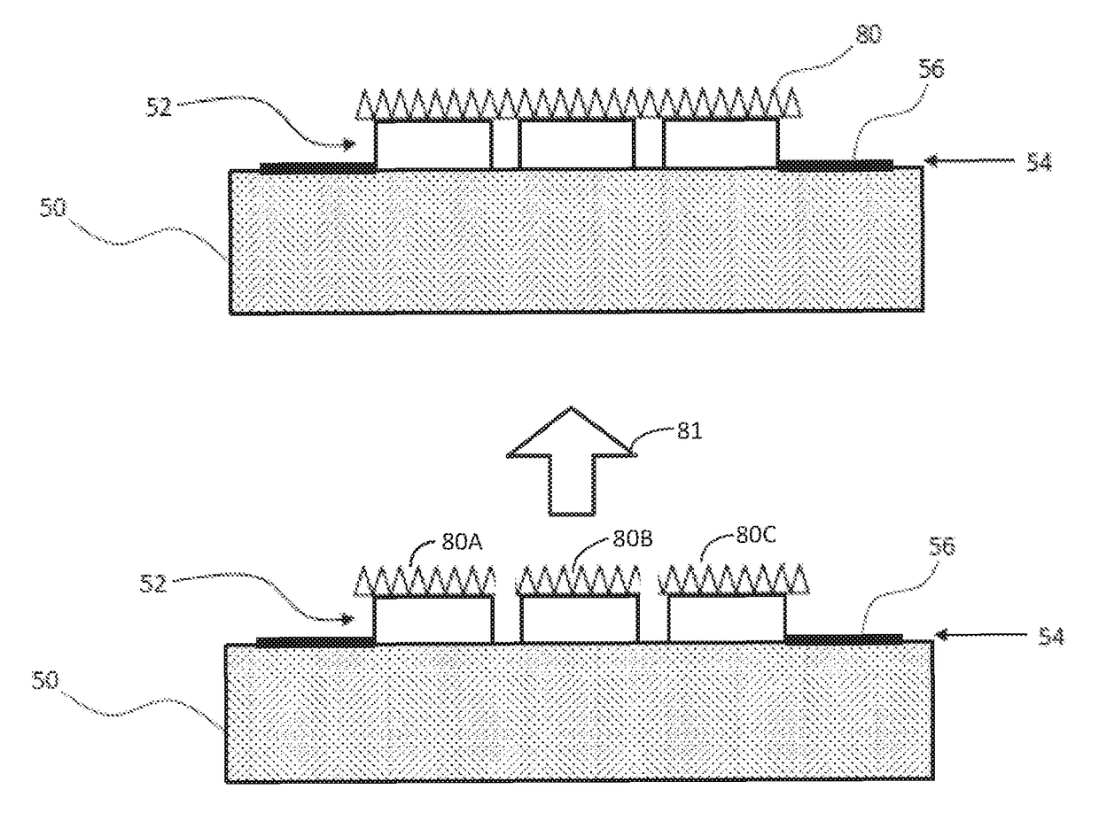
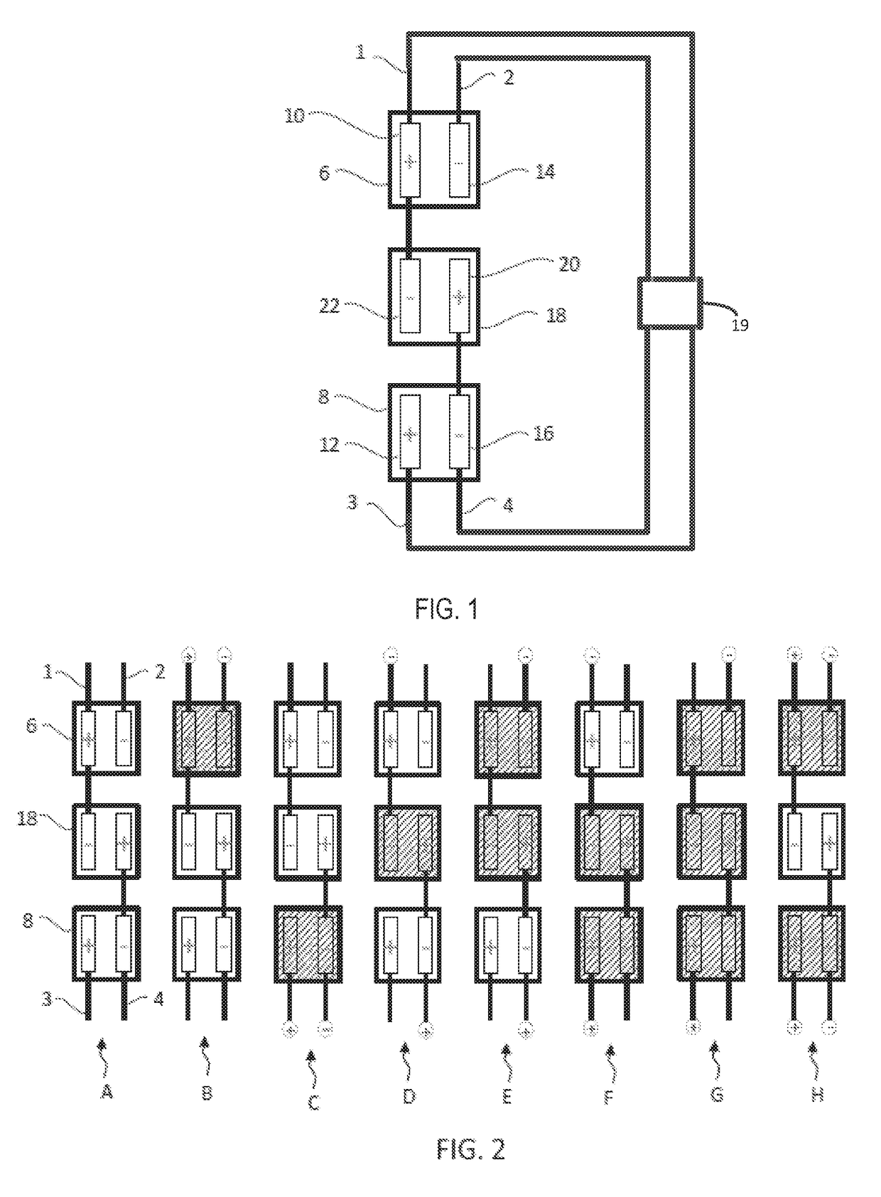
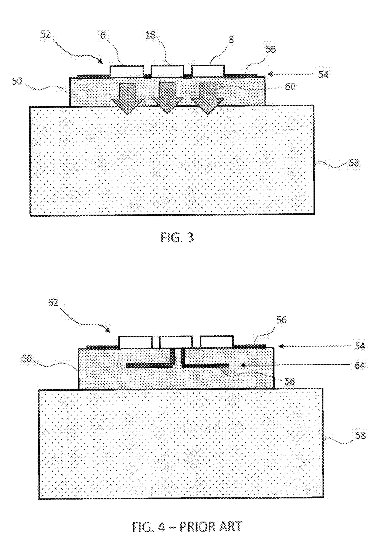
[0053]Aspects of the invention provide an interconnected string of three LED modules, having internal and external connections such that each LED in the string is fully individually addressable. LED biases and interconnects are oriented and configured such that individual addressability is achieved without the need for direct external signal connections to each LED in the string. Consequently embodiments are provided comprising pluralities of strings, arranged so as to form an array of LED modules, wherein wiring tracks running beneath, or along the intermediary spaces between, rows of LEDs are not required. Hence are provided LED devices comprising an array of individually addressable LED modules, having reduced spacing between rows and columns, and having optimal thermal path perpendicularly across the substrate layer. Provided devices have improved heat dissipation and greater achievable LED array density. Also provided are embodiments further comprising one or more beam-shaping ...


PUM


Abstract

The invention provides an interconnected string of three LED modules, having internal and external connections such that each LED in the string is fully individually addressable. LED biases and interconnects are oriented and configured such that individual addressability is achieved without the need for direct external signal connections to each LED in the string. Consequently embodiments are provided comprising pluralities of strings, arranged so as to form an array of LED modules, wherein wiring tracks running beneath, or along the intermediary spaces between, rows of LEDs are not required. Hence are provided LED devices comprising an array of individually addressable LED modules, having reduced spacing between rows and columns, and having optimal thermal path perpendicularly across the substrate layer. Provided devices have improved heat dissipation and greater achievable LED array density. Also provided are embodiments comprising one or more lens arrangements, suitable, for example, for adaptive beam-shaping applications.

Description

CROSS-REFERENCE TO RELATED APPLICATIONS[0001]The present application is a § 371 application of International Application No. PCT / EP2015 / 076459 filed on Nov. 12, 2015 and entitled “LED DEVICE HAVING INDIVIDUALLY ADDRESSABLE LED MODULES”, which claims the benefit of European Patent Application No. 14193989.2 filed on Nov. 20, 2014. International Application No. PCT / EP2015 / 076459 and European Patent Application No. 14193989.2 are incorporated herein.FIELD OF THE INVENTION[0002]The invention relates to an LED lighting unit adapted for individual addressability of LEDs.BACKGROUND OF THE INVENTION[0003]Light emitting diodes (LEDs) are increasingly used for a variety of lighting applications—and in particular are increasingly employed within automotive front lighting. LEDs offer a number of advantages over traditional (incandescent or fluorescent) light sources, including long lifetime, high lumen efficiency, low operating voltage and fast modulation of lumen output.[0004]LEDs also open up...

Claims


Application Information

Patent Timeline
Patent Type & Authority Patents(United States)
IPC IPC(8): H05B37/02H01L33/58H05B33/06H05B33/08H01L33/62H01L33/38H01L33/64F21W107/10H05B44/00
CPCH05B33/0827H01L33/387H01L33/58H05B33/083H01L33/642H05B33/06H01L33/62F21S41/141F21S41/285H01L25/0753H01L2924/0002F21W2107/10F21S45/47F21S41/19F21W2102/00F21S2/005F21S4/00F21Y2115/10F21V23/001F21S41/29H05B45/44F21S41/153H01L2924/00F21V29/70F21S41/00F21S10/023H05B45/46H05B45/48
Inventor KUMS, GERARD
Owner KONINKLJIJKE PHILIPS NV
Learn More