
Improvement for packing image sensing chip construction oncircuit board

A technology of image sensing and packaging methods, which is applied in the direction of circuits, color TV parts, TV system parts, etc., can solve problems such as the decline of good rate, the decline of product good rate, and the loss of foundries, so as to reduce the packaging process cost, the effect of reducing packaging steps

Inactive Publication Date: 2007-06-20
ACME SYST TECH CORP
View PDF0 Cites 4 Cited by
  • Summary
  • Abstract
  • Description
  • Claims
  • Application Information

AI Technical Summary

Problems solved by technology

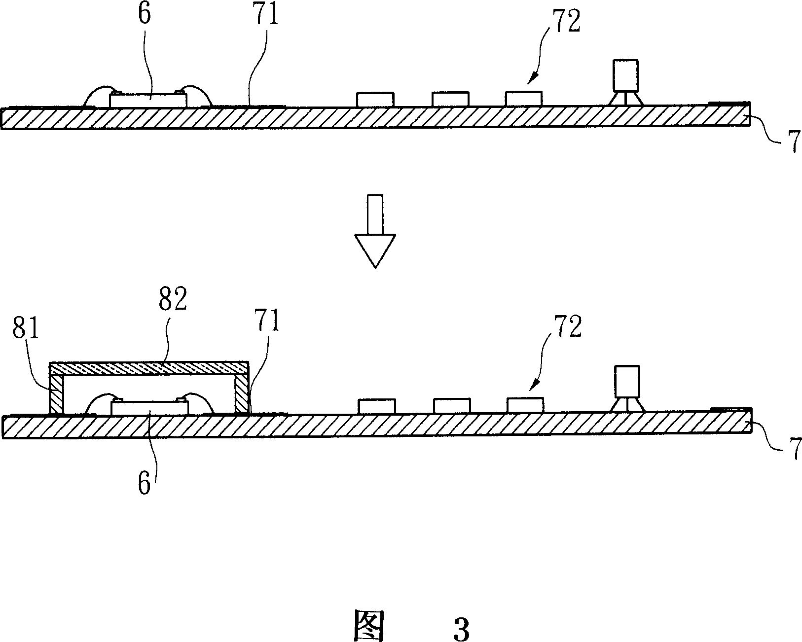
[0003] However, it can be found that the good rate of the above-mentioned image capture module B packaging product will often drop a lot when it passes the quality control and final imaging function test. After exploring the reason, it is found that the surface of the glass plate 82 may be contaminated with too much dust. And interfere with the imaging signal received on the image sensing chip 6
Inquiring into the source of contamination on the surface of the glass plate 82, it was found that it occurred during the transportation of the pre-packaged image sensor to the next foundry. As a result, the excellent rate of products decreased
[0004] The cost losses caused by these defective products are usually attributed to the foundry. However, the profit of the foundry is far less than the cost of the entire image sensor material. loss
In addition, the final imaging function test of the image capture module is to test out defective products after the entire image capture module is packaged. Therefore, it is not easy to detect image sensor modules with imaging defects during the packaging process.

Method used


Image

  • Improvement for packing image sensing chip construction oncircuit board
  • Improvement for packing image sensing chip construction oncircuit board
  • Improvement for packing image sensing chip construction oncircuit board

Examples


Embodiment Construction

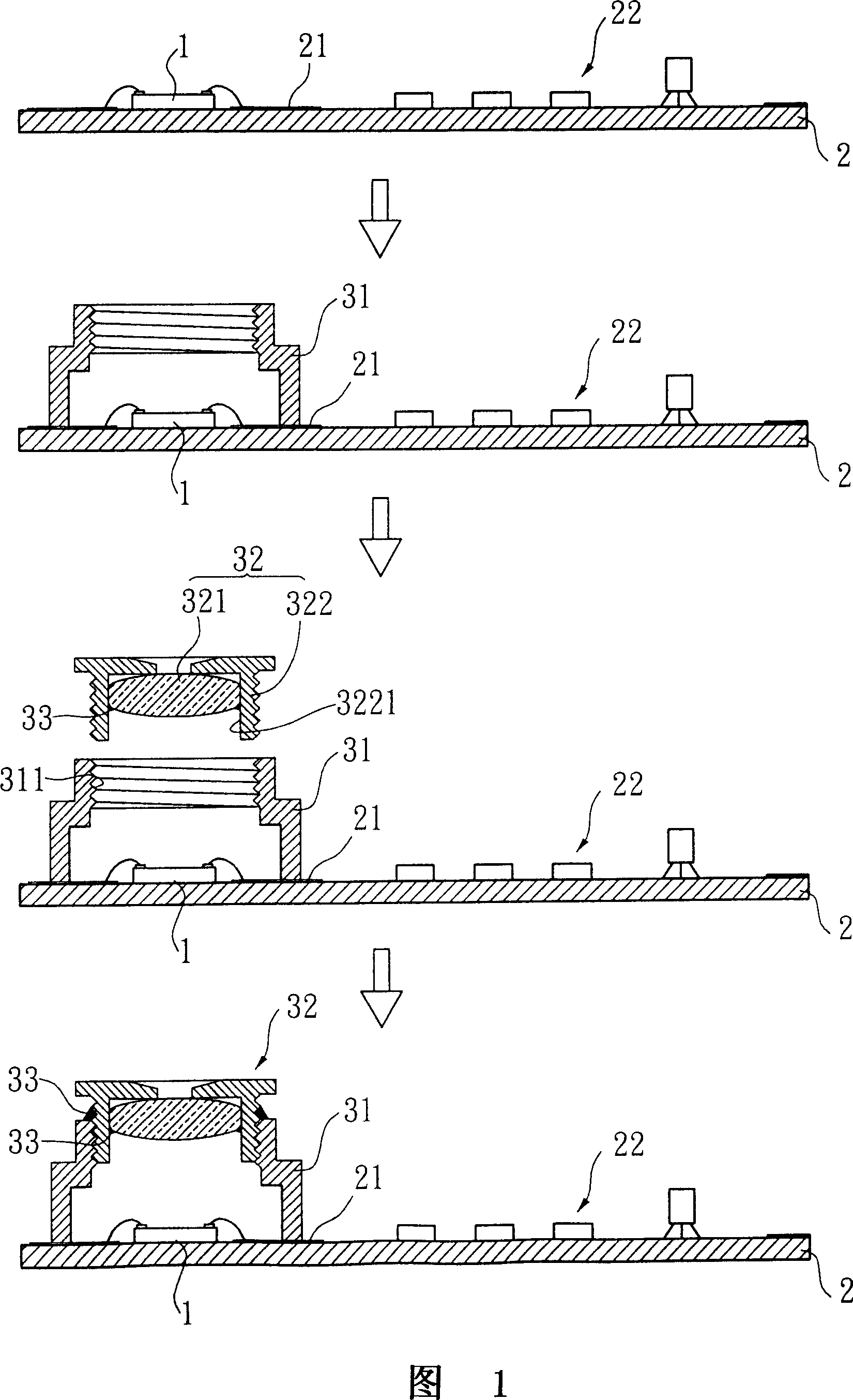
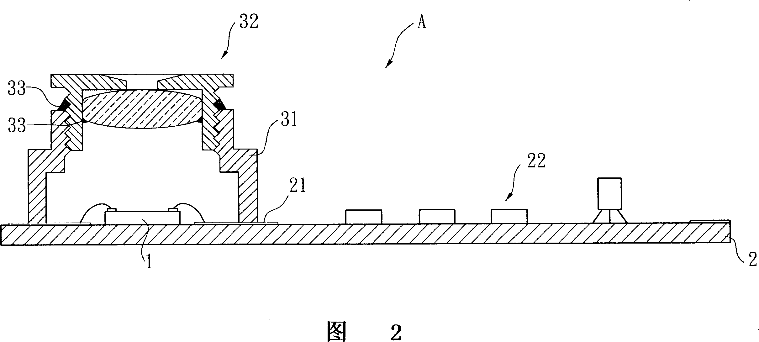
[0018] As shown in Fig. 1 and Fig. 2, the packaging method for improving the structure of the image sensor chip on the circuit board disclosed by the present invention includes the following steps:

[0019] First provide a module circuit substrate 2 with several pins 21 and module circuits 22 on the surface, and install an image sensing chip 1 on it, and wire from the image sensing chip 1 to each pin 21 to form an electrical circuit board. sexual connection.

[0020] A lens holder 31 is provided, and the lens holder 31 corresponds to the position of the image sensing chip 1 .

[0021] One or more lenses 321 are assembled into a slotted hole 3221 formed axially inside a cylindrical frame 322, and the gap between the periphery of the lens 321 and the wall of the slotted hole 3221 is filled with adhesive material 33 to seal the two to form a lens Assembly 32 , then, assemble the lens assembly 32 into the threaded hole 311 on the upper end of the lens mount 31 , so that the lens ...


PUM


Abstract

The invention is concerned with the encapsulation method that can improve image sensing wafer structured on the circuit board, it is: provides a module group circuit base-board that the surface of it is with numbers of pin and module group circuit, sets a image sensing wafer, the line of the image sensing wafer forms electrical connection with each pin; covers a camera lens base on the top of the image sensing wafer, glues on the circuit base-board; sets the camera lens groupware within a lens on the top of the camera lens base, adjusts the focus between the lens and the image sensing wafer; seals the camera lens groupware by the pastern and forms aeroseal at the joint part of the camera lens base, finishes the encapsulation of the image getting module.

Description

technical field [0001] The invention relates to a packaging method for improving the structure of an image sensing chip on a circuit board, especially to a method of directly using a lens group cover to be placed on the image sensing chip, omitting the original protection of the image sensing chip and placing it on it. The upper glass plate, thereby effectively reducing the chance of contacting pollution sources during the packaging process and reducing the cost of the packaging process. Background technique [0002] As shown in FIG. 3 , the packaging method of the traditional image capture module is: an image sensor chip 6 is installed on a surface with a plurality of pins 71 and each pin 71 is connected to the circuit board 7 of the module circuit 72 Above, the image sensor chip 6 is electrically connected to each pin 71 through the lead wire on the circuit board; 82 is glued on the frame tyrant 81 to form an airtight and protective electrical connection between the image...

Claims


Application Information

Patent Timeline
Patent Type & Authority Applications(China)
IPC IPC(8): H01L21/50H01L25/16H01L27/146H04N5/225
CPCH01L2224/48091H01L2224/48227
Inventor 冯琛
Owner ACME SYST TECH CORP
Learn More