


Quick Research
Generate reliable direction feasibility study reports for your R&D in just a few steps.

Technical Q&A
Discover and master advanced knowledge NOW. Basics, ideas, possibilities, all at once.

Find Solutions
As an expert in R&D theories, this can generate solutions to your technical problems instantly.

Evaluate Feasibility
Analyze your overall solution with one click, know your potential R&D risks in advance.

Monitor Landscape
Get weekly tech updates, stay abreast of the latest tech innovations and key insights.
Method for etching metal layer of display panel
A display panel and metal layer technology, which is applied in the direction of electrical components, semiconductor/solid-state device manufacturing, circuits, etc., can solve the problems of increased process cost and large etching amount, and achieve the effect of improving chamfering
- Summary
- Abstract
- Description
- Claims
- Application Information
AI Technical Summary
Problems solved by technology
Method used
Image

Examples
Embodiment 1
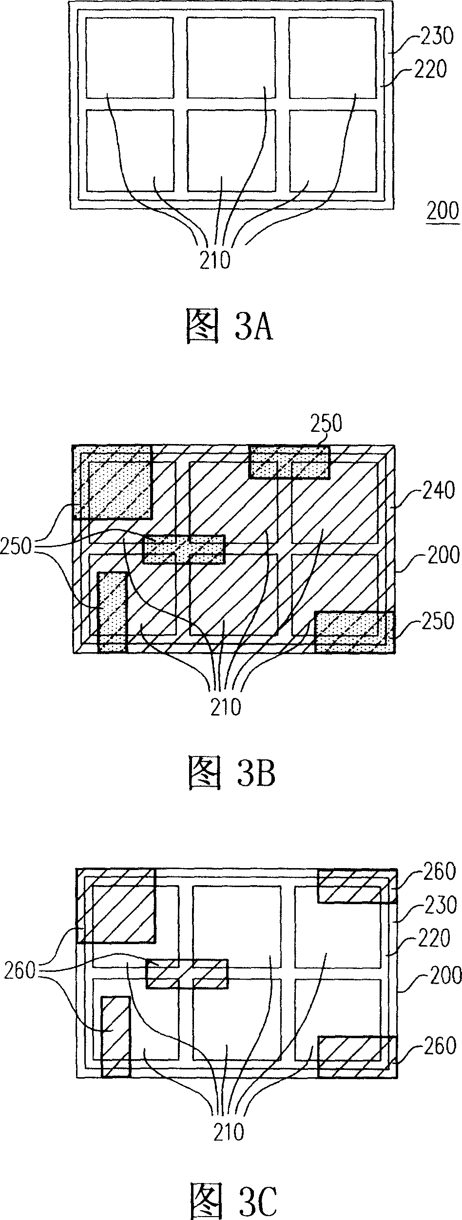
[0061] 3A to 3C are top views of the process flow of the etching method of the metal layer of the display panel according to an embodiment of the present invention. First, please refer to FIG. 3A , a substrate 200 is provided, and the substrate 200 is divided into several panel display areas 210 , a test component area 220 and a component-free area 230 .
[0062] In this embodiment, based on the area of the substrate 200, the area of several panel display areas 210 accounts for 81% of the area of the substrate 200, the test component area 220 accounts for 12% of the area of the substrate 200, and the non-component area 230 accounts for 81% of the area of the substrate 200. 7% of the area of the substrate 200 . The proportions of the regions in FIG. 3A are not the actual proportions on the substrate 200 , but are only used to represent the relative positions of the regions.
[0063] In this embodiment, the number of panel display areas 210 is 6 as an example, but i...
Embodiment 2
[0071]In this embodiment, the display panel used is substantially the same as that of the above embodiments, please refer to FIG. 3 , and details will not be repeated here. The biggest difference between this embodiment and the previous embodiments is that the design of the etching mask 250 is changed to increase the total exposed area of the metal layer 240 . As described below, if the total exposure ratio in this example is increased to (81%×80%)+(12%×80%)+(7%×80%)=80%, more aluminum can be exposed Metal. After performing the above etching process, the lateral etching rate of aluminum can be reduced to 25% to 60%, and the ratio of the maximum lateral etching amount to the minimum etching amount is further reduced to about 0.5 to 0.75. Under such a total exposure ratio, the chamfering phenomenon or the uneven lateral etching can be minimized, and the profile of the metal layer 240 will also be greatly improved.
[0072] Certainly, after performing the above metal layer et...
Embodiment 3
[0077] In another embodiment of the present invention, the design of the etching mask 250 is also used to increase the total exposure ratio of the metal layer 240 on the large-size panel to 72%. The etch rate is reduced by 10% to 30%, and the ratio of maximum lateral etch amount to minimum etch amount is reduced to 0.75 to 0.9. A good effect of improving the profile of the metal layer 240 can also be obtained.
PUM
 Abstract
Description
Claims
Application Information
 - R&D Engineer
- R&D Manager
- IP Professional
- Industry Leading Data Capabilities
- Powerful AI technology
- Patent DNA Extraction
Browse by: Latest US Patents, China's latest patents, Technical Efficacy Thesaurus, Application Domain, Technology Topic, Popular Technical Reports.
© 2024 PatSnap. All rights reserved.Legal|Privacy policy|Modern Slavery Act Transparency Statement|Sitemap|About US| Contact US: help@patsnap.com