Touch sensor and its manufacture method
A tactile sensor and tactile technology, applied in the field of tactile sensors, can solve problems such as low spatial resolution and difficult production, and achieve the effects of enhanced robustness, simple structure, and reduced cost
- Summary
- Abstract
- Description
- Claims
- Application Information
AI Technical Summary
Problems solved by technology
Method used
Image
Examples
Embodiment 1
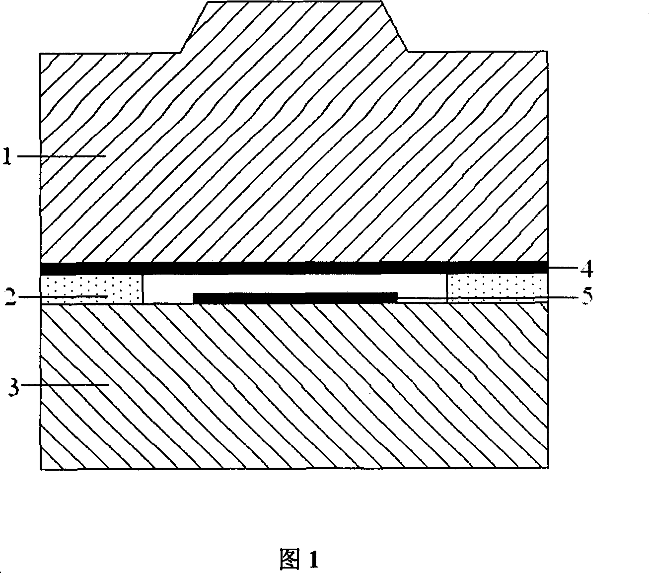
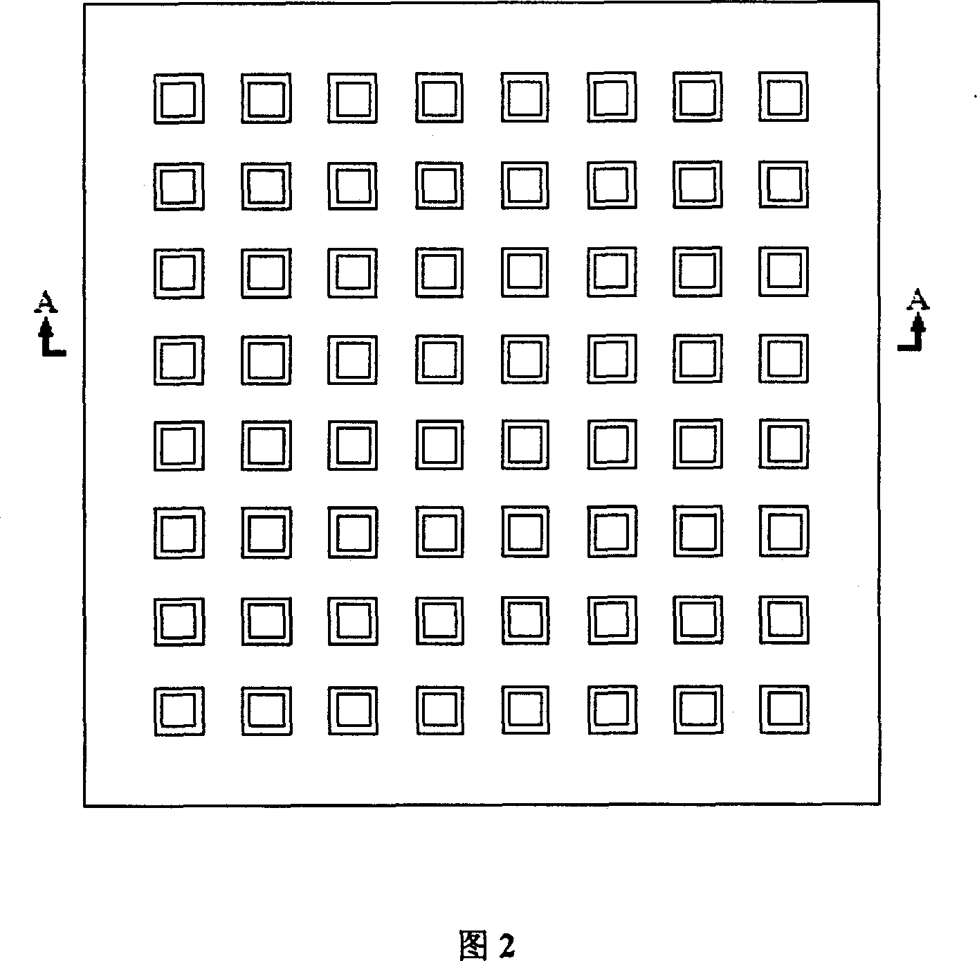
[0038] Referring to FIG. 2, FIG. 3, FIG. 4, and FIG. 5, this embodiment is a flexible switch type micro-tactile sensor with an array of 8×8 sensitive cells, including a tactile contact layer 1, a spacer layer 2, and a substrate layer 3. Both the tactile contact layer 1 and the substrate layer 3 are made of silicon rubber, and the material of the spacer layer 2 is polyimide. The upper surface of the tactile contact layer 1 has an array of 8×8 micro-protrusions, and each micro-protrusion is a sensitive point where the sensor contacts the object to be measured. The spacer layer 2 is located between the tactile contact layer 1 and the substrate layer 3 , and forms an 8×8 cavity array at the position corresponding to the micro-protrusions on the upper surface of the tactile contact layer 1 .
[0039] There are 8 rows of row electrodes 4 arranged in parallel on the direct contact surface between the tactile contact layer 1 and the spacer layer 2, and 8 rows of column electrodes 5 ar...
Embodiment 2
[0054] Referring to FIG. 6 and FIG. 7 , this embodiment is a flexible switch micro-tactile sensor with 7×10 sensitive cell arrays, including a tactile contact layer 1 , a spacer layer 2 , and a substrate layer 3 . The materials of the tactile contact layer 1 , the spacer layer 2 and the substrate layer 3 are all polyimide. The upper surface of the tactile contact layer 1 has a 7×10 micro-protrusion array, and each micro-protrusion is a sensitive point where the sensor contacts the object to be measured. The spacer layer 2 is located between the tactile contact layer 1 and the substrate layer 3 , and forms a 7×10 cavity array at the position corresponding to the micro-protrusions on the upper surface of the tactile contact layer 1 . There is a concave ring around the periphery of each micro-protrusion, and the structure of the concave ring makes the micro-protrusion easier to deform, thereby improving the sensitivity.
[0055] On the direct contact surface of the tactile conta...
PUM
 Abstract
Description
Claims
Application Information
 - R&D Engineer
- R&D Manager
- IP Professional
- Industry Leading Data Capabilities
- Powerful AI technology
- Patent DNA Extraction
Browse by: Latest US Patents, China's latest patents, Technical Efficacy Thesaurus, Application Domain, Technology Topic, Popular Technical Reports.
© 2024 PatSnap. All rights reserved.Legal|Privacy policy|Modern Slavery Act Transparency Statement|Sitemap|About US| Contact US: help@patsnap.com


