Analog to digital signal conditioning in optoelectronic transceivers

An optoelectronic transceiver, analog signal technology, applied in electromagnetic transceivers, electrical components, electromagnetic wave transmission systems, etc., can solve problems such as adverse effects of measurement accuracy

Inactive Publication Date: 2007-05-09
FINISAR
View PDF2 Cites 4 Cited by
  • Summary
  • Abstract
  • Description
  • Claims
  • Application Information

AI Technical Summary

Problems solved by technology

[0026] Device-to-device and production-lot variations of components within fiber optic transceivers can adversely affect the accuracy of measurements made to monitor operating conditions within the transceiver unless compensated for

Method used


Image

  • Analog to digital signal conditioning in optoelectronic transceivers
  • Analog to digital signal conditioning in optoelectronic transceivers
  • Analog to digital signal conditioning in optoelectronic transceivers

Examples


example 1

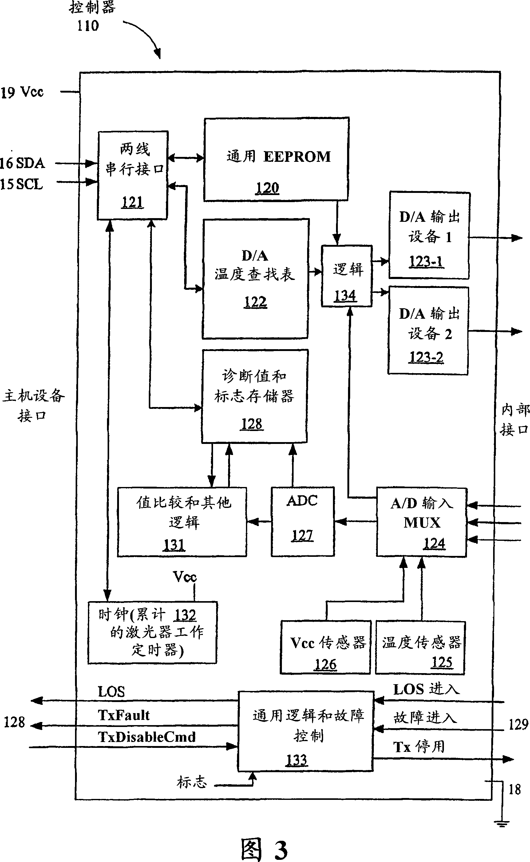
[0092] The power monitor 422 (FIG. 4) in the fiber optic transceiver includes the power monitor or its associated circuitry, and when it fails, it will indicate no or very low power output even if the laser is operating. The laser bias driver will attempt to increase the output power of the transmitter by increasing the laser bias current. Since the feedback is interrupted, the laser is driven to its maximum emission capability, which may exceed the eye safety alarm set point. A fast-trip alarm flag is generated within 10 microseconds of the fault and is used to shut down the laser driver via the internal Tx disable (Dout) output. A high-resolution alarm for laser bias current is generated and a high-resolution low alarm for power is also present if the fast-trip alarm fails or is not selected in the output logic settings, and either Both can be used to shut down the laser driver and / or TOSA.

example 2

[0094] When the laser driver (in all types of fiber optic transceivers) or its associated circuitry fails, the laser will be driven to its maximum output. Depending on the particular fault, the laser's bias current reading may be zero or very high, and, in fiber optic transceivers that include a power monitor, the power reading will be high. Within 10 microseconds, a fast-trip alarm for laser bias current and a fast-trip alarm for transmitted output power will generate an alarm flag. A high-resolution low alarm for laser bias current will generate an alarm flag if the laser bias current reading is zero. This may not be distinguishable from faults that result in zero light output (such as an open circuit in the laser line or a short circuit in the laser), however, safety considerations allow the alarm system to err on the side of this and command the laser to shut down. In this case, the logic cannot physically shut down the laser if the failure is caused by a shorted bias dri...


PUM


Abstract

Circuitry for monitoring the operation of an optoelectronic transceiver includes a sequence of interconnected signal processing circuits for processing an analog input signal and producing a digital result signal, where the analog signal represents one or more operating conditions of the optoelectronic transceiver. The sequence of signal processing circuits include gain circuitry for amplifying or attenuating the analog input signal by a gain value to produce a scaled analog signal, an analog to digital converter for converting the scaled analog signal into a first digital signal, and digital adjustment circuitry for digitally adjusting the first digital signal to produce the digital result signal. The digital adjustment circuitry includes shifting circuitry configured to shift an input digital signal in accordance with a shift value so as to produce a digital shifted signal. The digital result signal is stored in memory in predefined locations accessible by a host.

Description

[0001] This application is the U.S. Patent No. 09 / 777917 filed on February 5, 2001 entitled "INTEGRATED MEMORY MAPPED CONTROLLER CIRCUIT FOR FIBER OPTICS TRANSCEIVERS" and the 2002 Continuation-in-Part of US Patent Application Serial No. 10 / 266869, filed October 8, the entire contents of which are hereby incorporated by reference. technical field [0002] This invention relates generally to the field of fiber optic transceivers, and more particularly to circuits for monitoring and controlling these transceivers. More specifically, the present invention relates to improving the precision and accuracy of analog-to-digital converters (ADCs) used to monitor operating parameters within optoelectronic transceivers. Background technique [0003] The two most basic electronic circuits in the fiber optic transceiver are the laser drive circuit and the receiver circuit. The laser drive circuit receives high-speed digital data and drives the LED or laser diode electrically to generate ...

Claims


Application Information

Patent Timeline
Patent Type & Authority Applications(China)
IPC IPC(8): H04B10/08H04B10/28H04B10/02H04B10/43
CPCH04B10/07H04B10/43H04B2210/08H04B10/0799
Inventor L·B·阿伦森L·G·霍斯金D·卡斯J·C·哈欣G·L·迪布塞特
Owner FINISAR
Why Eureka
Try Eureka