
Multi-layer packaging structure and producing method thereof

A packaging structure, multi-level technology, applied in the direction of semiconductor devices, electrical components, circuits, etc., can solve the oxidative discoloration of phosphor powder and large-scale light decay, but cannot provide a comprehensive and complete solution, light-emitting diode oxidative discoloration, light decay level increase problem

Inactive Publication Date: 2007-01-03
周志邦
View PDF0 Cites 3 Cited by
  • Summary
  • Abstract
  • Description
  • Claims
  • Application Information

AI Technical Summary

Problems solved by technology

However, in the above-mentioned LED packaging structure, the direct contact between the LED and the phosphor film will cause the LED to oxidize and discolor due to high temperature due to long-term light emission, and gradually reduce the overall brightness of the LED, resulting in light decay. Greatly increased, thereby shortening the service life of light-emitting diodes
[0003] In the prior art, relative to the packaging structure of the light emitting diode, the light emitting diode directly contacts the phosphor powder, but it may not be able to provide a comprehensive and complete solution for the oxidative discoloration and large-scale light decay of the phosphor powder.

Method used

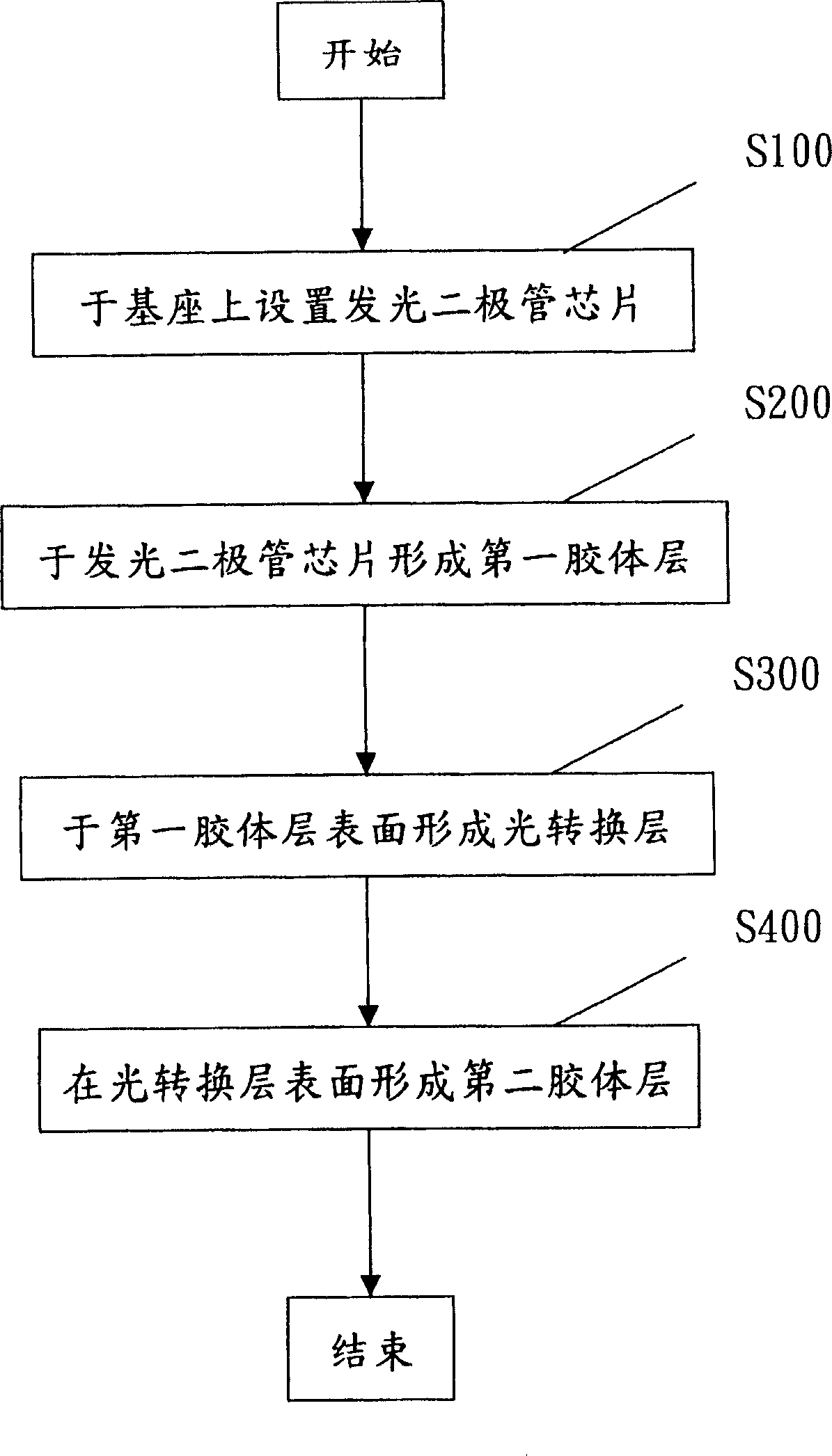
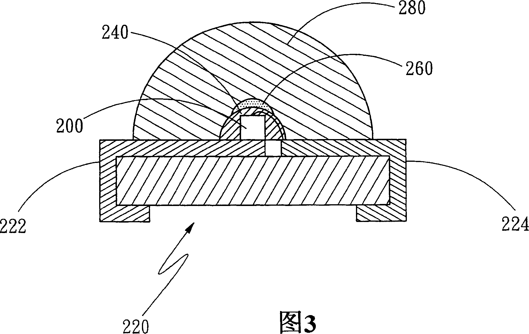

Image

  • Multi-layer packaging structure and producing method thereof
  • Multi-layer packaging structure and producing method thereof
  • Multi-layer packaging structure and producing method thereof

Examples


Embodiment Construction

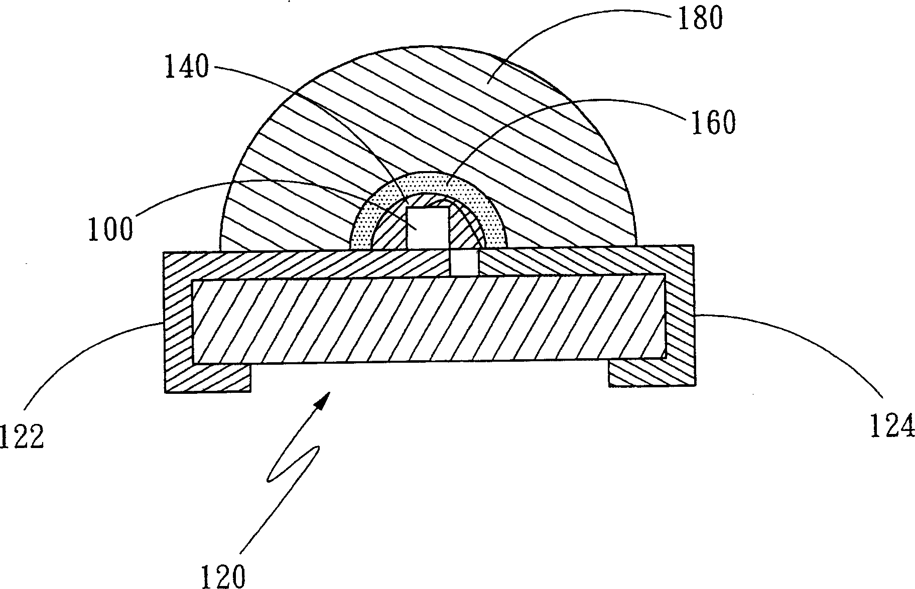
[0024] see figure 1 , figure 1 It is a sectional view of a preferred embodiment of the present invention. The present invention provides a multi-level packaging structure, which includes a light-emitting diode chip 100, which is arranged on the surface of a base 120, and the base 120 has a set of conductive circuits 122, 124, the conductive circuit 122, 124 transmit power to provide the light-emitting diode chip 100 to emit light, and an insulating material (not shown in the figure) is provided around the conductive lines 122, 124 to prevent the power from leaking out; a first colloidal layer 140 has light transmission , such as light-transmitting resin (EPOXY), used to coat the light-emitting diode chip 100; a light conversion layer 160, which can be spin-coated, sputtered, printed, The surface of the first colloidal layer 140 is completely covered by liquid droplets, formed first and then bonded, or other similar methods, and the light conversion layer 160 contains at leas...


PUM


Abstract

The present invention relates to a multilayer packaging structure, light conversion particle and luminous element in its division light conversion layer. Luminous element generated high temperature does not make directly light conversion particle oxidative stain, therefore capable of effectively reducing current luminous element light decline phenomena generated by high temperature heating for a long time, and then prolonging said multilayer packaging structure illuminator service life.

Description

technical field [0001] The invention relates to a multi-level packaging structure and a manufacturing method thereof, in particular to a method for separating a light-emitting diode chip and a light conversion layer to prevent the high heat generated by the light-emitting diode chip from causing oxidation and discoloration of the light conversion layer. Background technique [0002] Most of the existing white light emitting diode (LED, Light Emitting Diode) packaging structures use blue light emitting diodes to excite phosphor powder to emit yellow light. After mixing the two kinds of light, blue light and yellow light can visually form white light. However, since the white color produced by existing white light emitting diodes is a mixture of blue light and yellow light, it is difficult to completely control the light emitted by white light emitting diodes into pure white, and most of them are white with blue or yellow halos. That means white light emitting diodes have non-...

Claims


Application Information

Patent Timeline
IPC IPC(8): H01L33/00H01L33/48H01L33/62
CPCH01L2224/8592H01L2924/181H01L2224/48091H01L2224/48247H01L2924/00014H01L2924/00012
Inventor 周志邦
Owner 周志邦
Learn More