Display apparatus having active matrix display panel, and method for driving the same

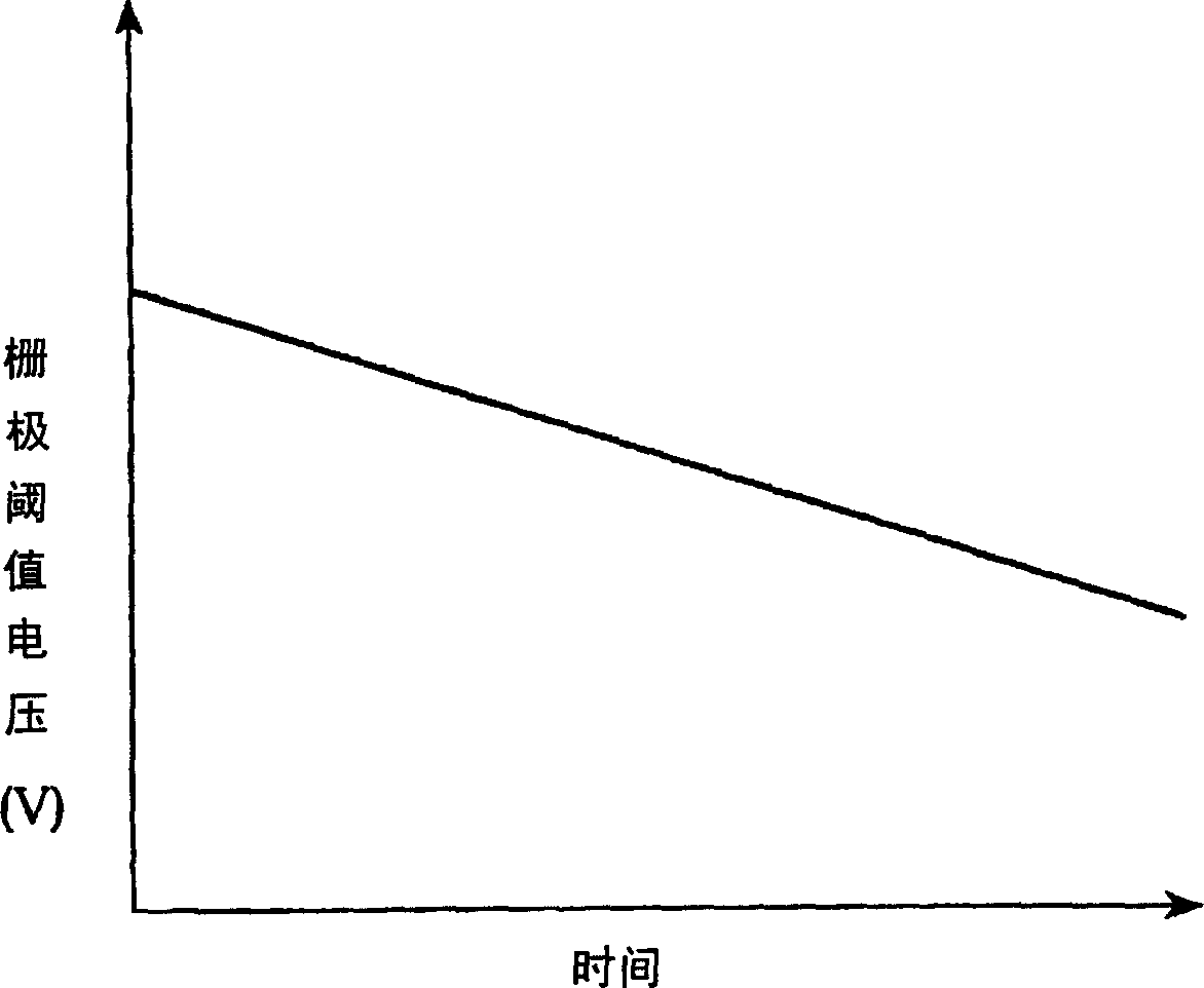
A display device and display panel technology, which is applied to static indicators, instruments, etc., can solve the problems of large drive current error, display quality, drive voltage increase, power consumption increase, etc.

Inactive Publication Date: 2006-11-15
PIONEER CORP
View PDF0 Cites 15 Cited by
  • Summary
  • Abstract
  • Description
  • Claims
  • Application Information

AI Technical Summary

Problems solved by technology

[0003] In the existing driving method, in addition to the deviation of the initial value of Vth, it is necessary to estimate the variation of Vth caused by the gate stress to set the driving voltage and driving conditions, so the driving voltage will increase, resulting in power consumption. increase
In addition, as the Vth deviation increases, even if a circuit that corrects this deviation is used, the error of the drive current will increase and the display quality will deteriorate.

Method used


Image

  • Display apparatus having active matrix display panel, and method for driving the same
  • Display apparatus having active matrix display panel, and method for driving the same
  • Display apparatus having active matrix display panel, and method for driving the same

Examples


Embodiment Construction

[0021] Embodiments of the present invention will be described below with reference to the drawings.

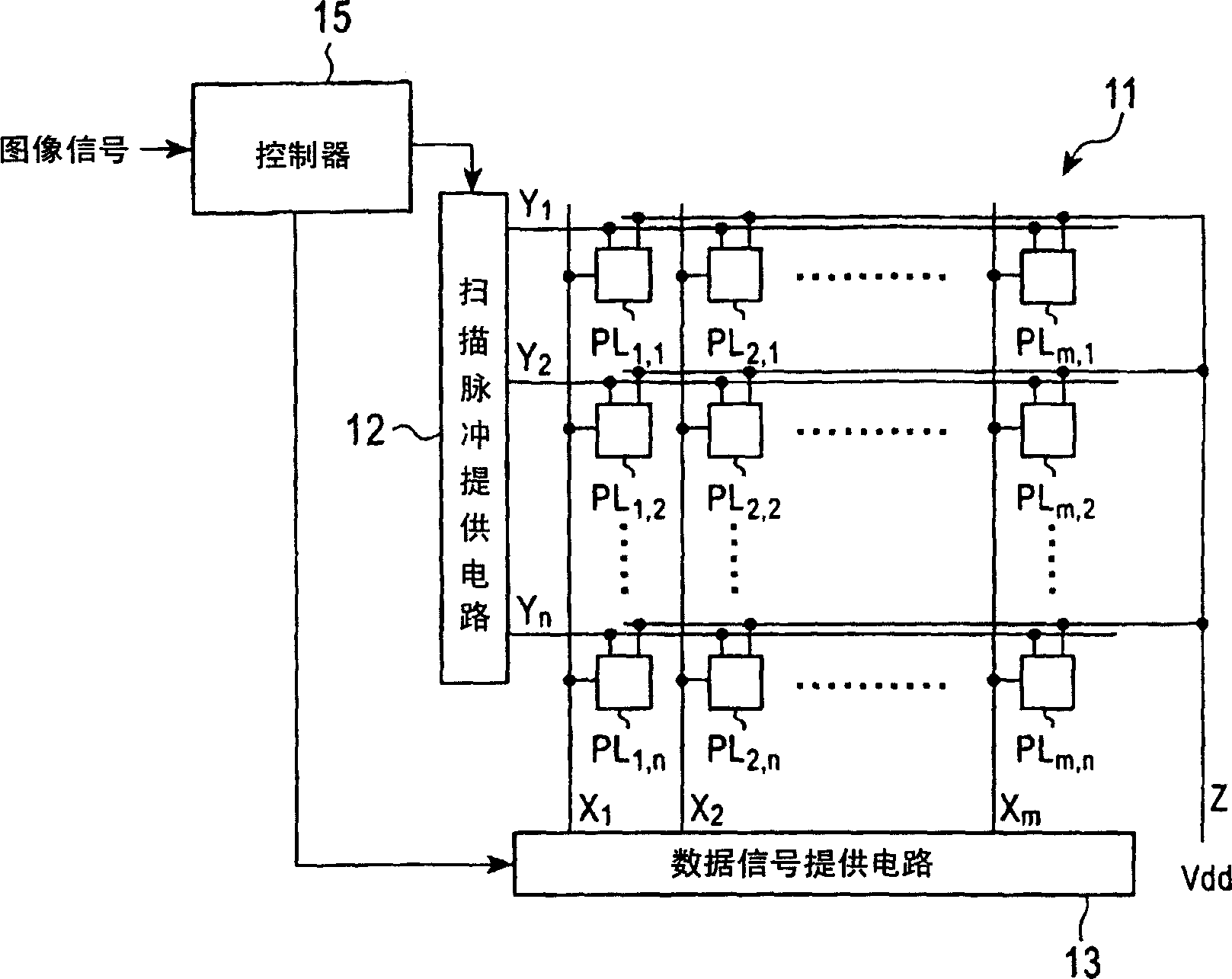
[0022] figure 2 A display device using the active matrix display panel of the present invention is shown. The display device includes a display panel 11 , a scan pulse supply circuit, a data signal supply circuit 13 and a controller 15 .

[0023] The display panel 11 is an active-matrix display panel composed of m×n pixels (m and n are integers greater than 2), and includes a plurality of data lines X1 to Xm and a plurality of scanning lines Y1 to Y arranged in parallel. Yn and multiple pixel units PL 1,1 ~PL m,n . pixel unit PL 1,1 ~PL m,n They are arranged at intersections of the data lines X1 to Xm and the scanning lines Y1 to Yn, and all have the same structure. In addition, the pixel unit PL 1,1 ~PL m,n Connect to power cord Z. A power supply voltage (positive voltage Vdd) is supplied to the power supply line Z from a power supply (not shown).

[0024] As show...


PUM


Abstract

A display apparatus having an active matrix display panel, and a method for driving the same, wherein the gate stress can be suppressed to prevent degradation of display quality. A data pulse indicative of a first gate voltage of each film transistor is supplied to a respective one of the pixel parts of a row during supply of a display scan pulse. Thereafter, a reset scan pulse is supplied to the pixel parts of the row, and a reset pulse indicative of a second gate voltage of the film transistor is supplied to the respective one of the pixel parts of the row during supply of the reset scan pulse so as to cause the gate-source voltage of the film transistor to have an opposite polarity to that during light emission driving.

Description

technical field [0001] The present invention relates to a display device including an active matrix display panel and a driving method thereof. Background technique [0002] In an active matrix display using a light emitting element, a TFT (Thin Film Transistor: thin film transistor) using polysilicon, amorphous silicon (a-Si), organic semiconductor, etc. is used as a driving element for each pixel. In TFTs using amorphous silicon or organic semiconductors, it is known that there is a phenomenon in which gate threshold voltage Vth shifts when a voltage is continuously applied to the gate, that is, gate stress (gate stress) (for example, refer to S.J.Zilker, Ch. . Detcheverry, E. Cantatore, and D.M. de Leeuw: APPLIED PHYSICSLETTERS VOLUME 79, NUMBER 8 20AUGUST 2001, "Bias stressin organic thin-film transistors and logic gates"). This phenomenon is illustrated by taking a P-channel TFT as an example. exist Figure 1A and Figure 1B The state of gate threshold voltage shift ...

Claims


Application Information

Patent Timeline
Patent Type & Authority Applications(China)
IPC IPC(8): G09G3/30G09G3/20G09G3/32
CPCG09G3/2022G09G3/3233G09G2300/0823G09G2300/0842G09G2300/0852G09G2310/0251G09G2310/0254G09G2320/043G09G3/20G09G3/30
Inventor 田边贵久
Owner PIONEER CORP
Why Eureka
Try Eureka