Touch input sensing device
A technology of touch sensing and touch sensor, which is applied in the field of capacitive sensing devices, and can solve the problems of affecting touch accuracy, insufficient protection of conductive films, and reduction of coating quality, etc.
- Summary
- Abstract
- Description
- Claims
- Application Information
AI Technical Summary
Problems solved by technology
Method used
Image
Examples
example 1
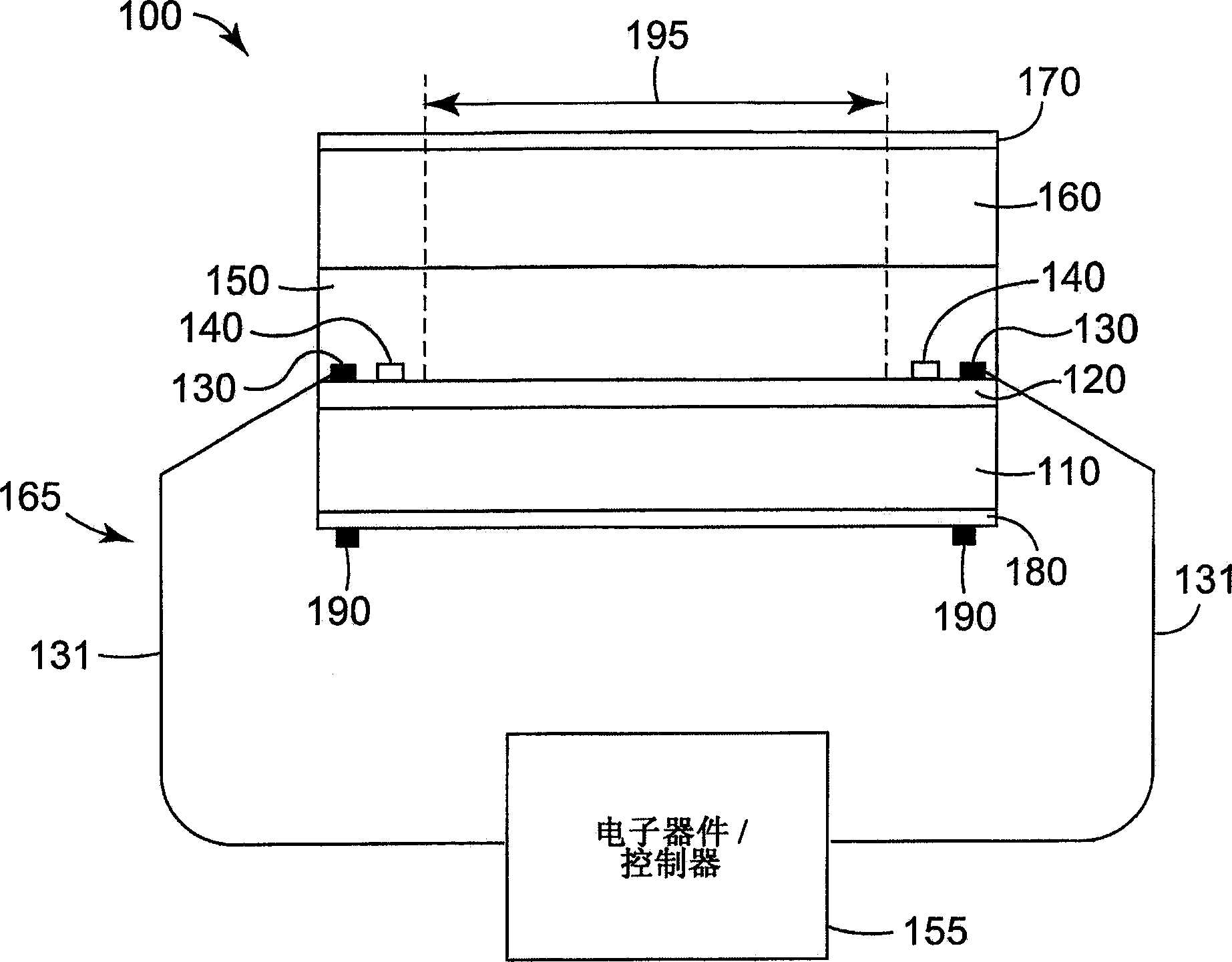
[0069] A touch sensor according to one embodiment of the present invention is assembled as follows.
[0070] A 3 mm thick soda lime glass substrate was dip coated in a solution which may contain an organic conductive material commercially available from Baytron P under the trademark Baytron P. The solution also includes ethylene glycol and epoxy silane coupling agents. The solution was diluted with isopropanol. Both sides of the glass substrate were coated by dipping treatment. The coated glass substrate was dried and cured at 85° C. for 6 minutes, thereby obtaining a conductive polymer film formed on both sides of the glass substrate.
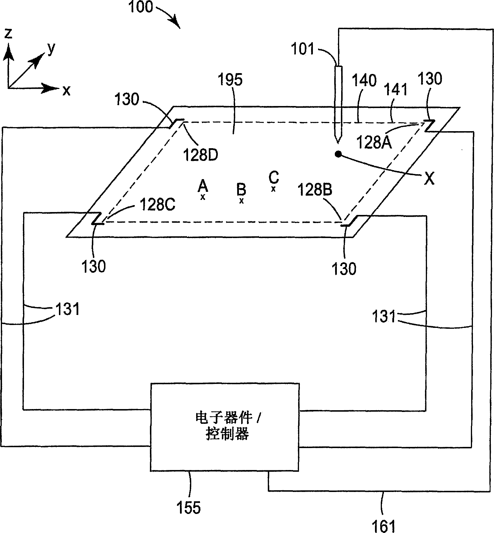
[0071] Next, along the perimeter of one side of the panel, a linearization structure was screen printed using carbonized conductive ink. The printed substrates were cured at 130°C for 6 minutes.
[0072] Next, use conductive epoxy to electrically connect wires to the four corners of the linearization structure. The assembly was cured at 1...
example 2
[0077] A touch sensor according to one embodiment of the present invention was prepared similarly to Example 1, except that a 0.4 mm thick soda lime glass substrate was used for dip coating. Use the Controller EX II to activate the finished assembly. The results of the finger-drawing test were linear better than 1%.
example 3
[0079] A touch sensor according to one embodiment of the present invention is assembled as follows.
[0080] Linearization structures were screen printed along the perimeter on one side of a 3 mm thick soda lime glass substrate and coated with 1500 ohms / unit area of TAO on the same side. The conductive ink used to print the linearization structures was from DuPont under the trade mark 7713. The printed substrates were cured at 500°C for 15 minutes.
[0081] Next, wires were connected to the four corners of the linear structure similarly to Example 1.
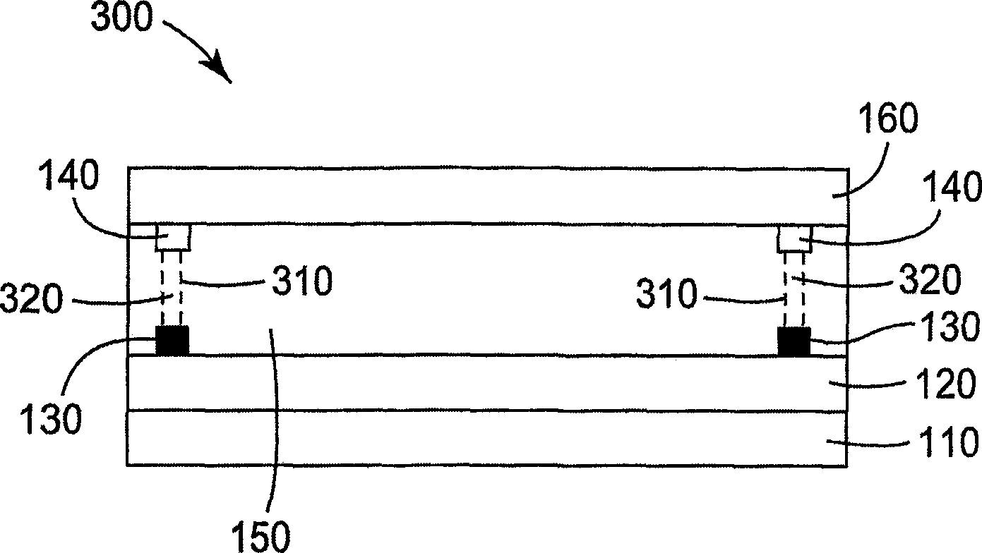
[0082] Next, 0.4 mm thick soda lime glass was glued to this side of the panel printed with the linearized structure. Bonding was accomplished using an optical adhesive from Norland Corporation under the trade mark NOA 68. The adhesive is cured using ultraviolet light.
[0083] Next, activate the finished assembly using the EX II controller connected to the wires. The results of the finger-drawing test were linear better t...
PUM
 Abstract
Description
Claims
Application Information
 - R&D
- Intellectual Property
- Life Sciences
- Materials
- Tech Scout
- Unparalleled Data Quality
- Higher Quality Content
- 60% Fewer Hallucinations
Browse by: Latest US Patents, China's latest patents, Technical Efficacy Thesaurus, Application Domain, Technology Topic, Popular Technical Reports.
© 2025 PatSnap. All rights reserved.Legal|Privacy policy|Modern Slavery Act Transparency Statement|Sitemap|About US| Contact US: help@patsnap.com


