Epitaxial structure for vertical cavity emitting semiconductor laser diode

A technology of vertical cavity surface emission and laser diodes, which is applied in the direction of semiconductor lasers, lasers, laser components, etc., to achieve the effects of good stability, high repeatability, and simple manufacturing process

Inactive Publication Date: 2006-10-18
ADVANCED OPTRONIC DEVICES CHINA
View PDF0 Cites 4 Cited by
  • Summary
  • Abstract
  • Description
  • Claims
  • Application Information

AI Technical Summary

Problems solved by technology

However, there are many bottlenecks in the preparation of vertical cavity surface emitting semiconductor lasers. If you want to further mass produce, you still need to overcome the problems of materials, processes and yields, and provide new vertical cavity surface emitting semiconductor laser materials.

Method used


Image

  • Epitaxial structure for vertical cavity emitting semiconductor laser diode

Examples


Embodiment Construction

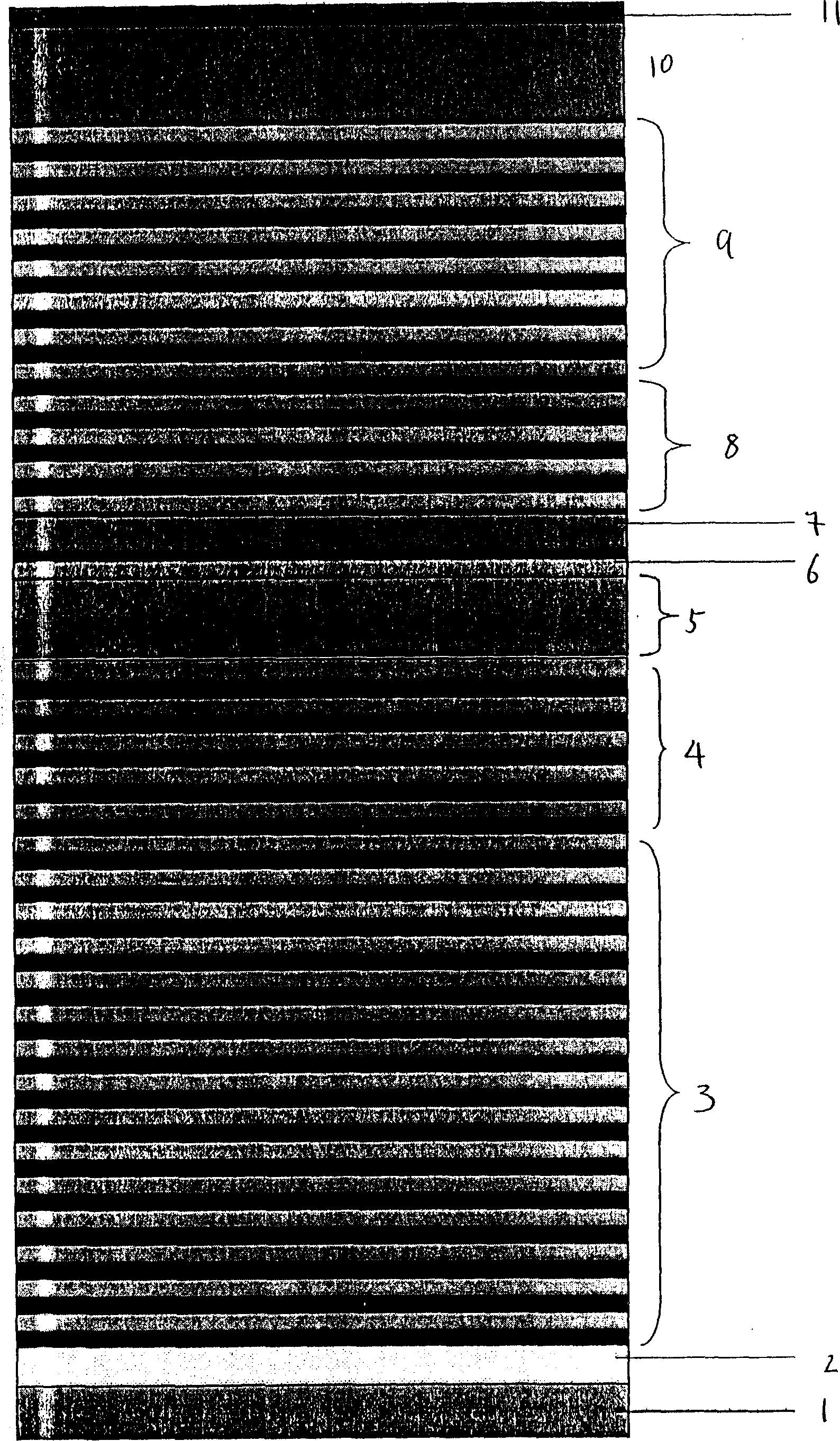
[0028] Referring to the accompanying drawings, the epitaxial structure of the vertical cavity surface emitting semiconductor laser diode includes the following eleven parts, each part is a layer structure, the part (1) is a (100) gallium arsenide substrate, and the crystal orientation deviation angle is 0.8-8 degree, the silicon doping concentration is 0.5-3×10 18 / cc. Part (2) is a grown single-layer gallium arsenide transition layer with a thickness of 3000-7000 Ȧ and a silicon doping concentration of 0.5-3×10 18 / cc. Part (3) is the growth of 30-40 layers of external N-type Bragg reflective layer, the reflective layer is composed of AlGaAs, the thickness conforms to the Bragg reflective definition, and the silicon doping concentration is 0.5-3×10 18 / cc. Part (4) is the growth of 5-10 layers of internal N-type Bragg reflective layer, the reflective layer is composed of AlGaAs, the thickness conforms to the Bragg reflective definition, and the silicon doping concentration...


PUM


Abstract

An epitaxial structure using vertical cavity surface to emit semiconductor laser diode consists of GaAs substrate, grown single- layer GaAs transition layer, grown multilayer external N type of Bragg reflection layer and internal N type of Bragg reflection layer, grown multilayer quantum well structure, grown single-layer internal P type of Bragg reflection layer, grown multilayer P type of oxidation layer, grown multilayer internal P type of reflection layer and external P type of Bragg reflection layer, grown single- layer high doped P type of current expansion layer and ground single-layer super high doped P type of surface covering layer.

Description

technical field [0001] The invention relates to a semiconductor laser material in the field of optical communication, in particular to an epitaxial structure of a vertical cavity surface emitting semiconductor laser diode. Background technique [0002] Vertical cavity surface emitting semiconductor laser is a semiconductor laser that emits light from the direction perpendicular to the surface of the semiconductor substrate. It has good mode, low threshold, good stability, long life, high modulation rate, high integration, small divergence angle, and coupling efficiency. High, cheap and many other advantages. Because multiple lasers can be arranged in parallel in the direction perpendicular to the substrate, it is very suitable for applications in the fields of parallel optical transmission and parallel optical interconnection. It has been successfully applied to single-channel and parallel optical interconnection at an unprecedented speed. It has a high performance-price ra...

Claims


Application Information

Patent Timeline
Patent Type & Authority Applications(China)
IPC IPC(8): H01S5/183H01S5/00H01S5/187H01S5/343
Inventor 蒋伟刘凯张彦伟孙夕庆
Owner ADVANCED OPTRONIC DEVICES CHINA
Why Eureka
Try Eureka