Wafer for evaluation, evaluation method and method of manufacturing semiconductor device

An evaluation method, semiconductor technology, applied in semiconductor/solid-state device manufacturing, semiconductor/solid-state device testing/measurement, electrical components, etc. Effect of small shot distribution deviations

Inactive Publication Date: 2006-10-18
RICOH KK
View PDF4 Cites 5 Cited by
  • Summary
  • Abstract
  • Description
  • Claims
  • Application Information

AI Technical Summary

Problems solved by technology

[0006] When the injection density ratio is 1.0×10 12 ions / cm 2 Small occasions, the method utilizing thermal waves can also measure the ion implantation amount, but there are limitations in using this method, generally only hundreds of points can be measured in the semiconductor wafer plane, and the ion implantation amount distribution in the semiconductor wafer plane cannot be measured in detail

Method used


Image

  • Wafer for evaluation, evaluation method and method of manufacturing semiconductor device
  • Wafer for evaluation, evaluation method and method of manufacturing semiconductor device
  • Wafer for evaluation, evaluation method and method of manufacturing semiconductor device

Examples


Embodiment Construction

[0052] Hereinafter, embodiments of the present invention will be described in detail with reference to the accompanying drawings. In the following embodiments, although various limitations are made on constituent elements, types, combinations, shapes, relative arrangements, etc., these are merely examples, and the present invention is not limited thereto.

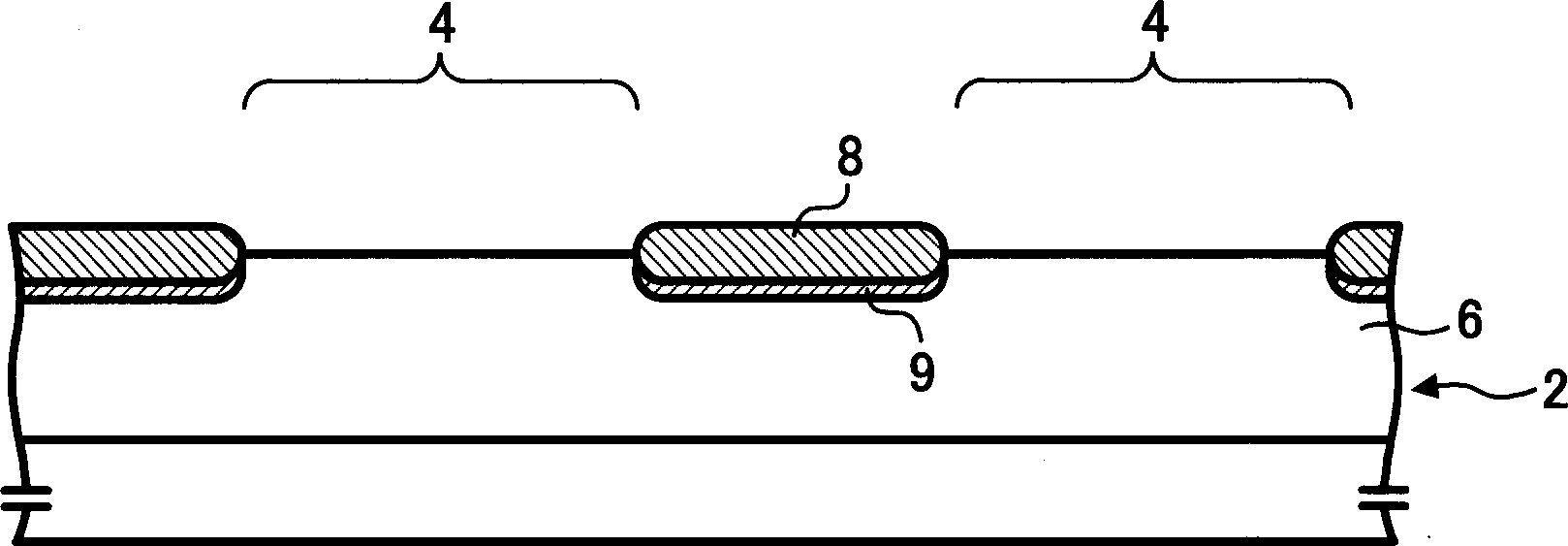
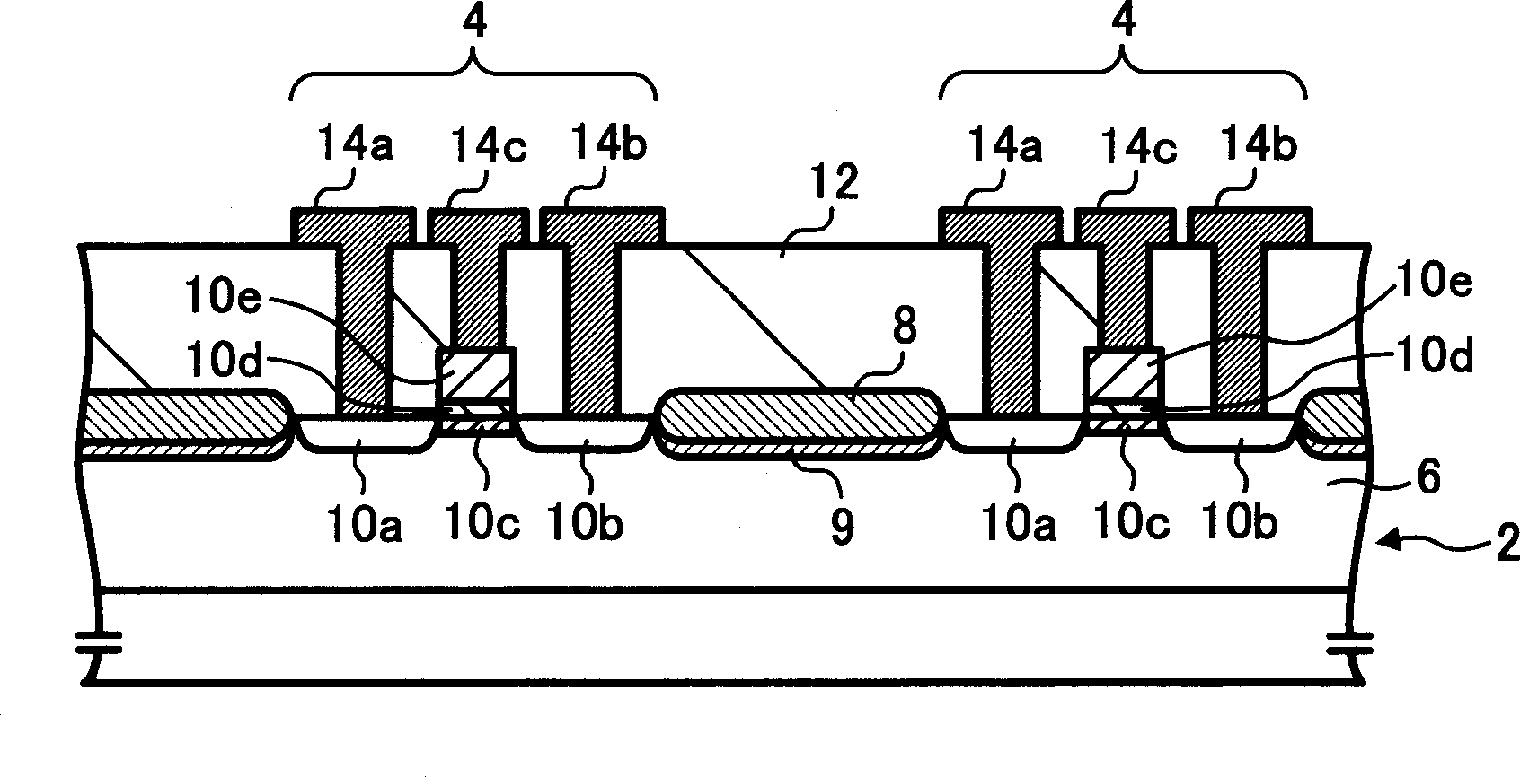
[0053] The wafer shown in this example is not a semiconductor wafer actually used for manufacturing a semiconductor chip, but an evaluation wafer for an ion implantation test used to evaluate the distribution deviation of the ion implantation amount in the main surface of the semiconductor wafer. In the present embodiment, the ion implantation to be evaluated is impurity implantation for threshold voltage control of transistors, which is hereinafter abbreviated as "channel doping".

[0054] figure 1 It is a cross-sectional view for explaining an example of a wafer for evaluation.

[0055] On the entire main surface of the...


PUM


Abstract

The present invention relates to a wafer for evaluation, a method for evaluating ion implantation amount distribution, and a method for manufacturing a semiconductor device. Using a wafer 2, a plurality of evaluation transistor formation regions 4 having the same impurity concentration are arranged in an equal-density distribution over the entire main surface of the wafer 2, and threshold voltage control is performed in the evaluation transistor formation regions 4 of the wafer 2. Impurity implantation, as the impurity implantation to be evaluated, formed evaluation transistors of the same structure in each evaluation transistor formation region 4, measured the threshold voltage of the evaluation transistors, and evaluated the evaluation transistors based on the threshold voltage distribution of the evaluation transistors. impurity concentration distribution in the main surface of the wafer. The amount of ion implantation is not limited, and the distribution of ion implantation amount in the semiconductor wafer surface can be evaluated in detail.

Description

technical field [0001] The present invention relates to a wafer for evaluation or inspection, and more specifically, to a wafer for evaluating ion implantation amount distribution, a method for evaluating ion implantation amount distribution, and a method for manufacturing a semiconductor device for evaluating when implanting ions into a semiconductor wafer. The resulting in-plane ion implantation amount distribution deviation. Background technique [0002] In order to reduce the size of the semiconductor chip, it is important to reduce the variation in the amount of ion implantation to a minute region within the surface of the semiconductor wafer by producing a product that utilizes analog characteristics. As a method of measuring ion implantation amount distribution (impurity concentration distribution) in the surface of a semiconductor wafer, for example, a method using sheet resistance, such as JP-A-10-172917 (hereinafter abbreviated as "Patent Document 1") is exemplifie...

Claims


Application Information

Patent Timeline
Patent Type & Authority Applications(China)
IPC IPC(8): H01L21/66H01L21/265
CPCH01L21/67253H01L22/26
Inventor 小国干典
Owner RICOH KK
Why Eureka
Try Eureka