Electroluminescent device and display

A technology of electric field luminescence and components, which is applied in the direction of electrical components, electroluminescent light sources, electric light sources, etc., can solve the problems of high cost of driving circuits, strong charge repulsion, etc., and achieve high brightness luminous efficiency, low voltage drive, and high luminous efficiency Effect

Inactive Publication Date: 2006-08-09
PANASONIC CORP
View PDF0 Cites 3 Cited by
  • Summary
  • Abstract
  • Description
  • Claims
  • Application Information

AI Technical Summary

Problems solved by technology

Therefore, although luminescence by ultraviolet light excitation is realized, on the other hand, even if an electric field is applied, it is difficult for electrons to permeate into the inorganic phosphor, and the charged repulsion is also strong, so it is necessary to impact and excite high-speed electrons accelerated by a high electric field Luminescent Centers in Inorganic Phosphors
Therefore, it is usually necessary to apply an AC voltage of hundreds of volts at a high frequency of several kHz, which raises the cost of the drive circuit.

Method used


Image

  • Electroluminescent device and display
  • Electroluminescent device and display
  • Electroluminescent device and display

Examples


Embodiment approach 1

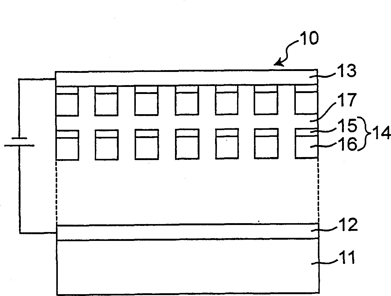
[0047] control figure 1 The electroluminescence element related to Embodiment 1 of the present invention will be described. figure 1 This is a cross-sectional view illustrating the structure of the electroluminescent element 10 according to the first embodiment. The electroluminescent device 10 has a multilayer structure, and has a pair of anode electrodes 12 and cathode electrodes 13 facing each other on a substrate 11 . In addition, between the anode electrode 12 and the cathode electrode 13 , a light emitting layer 14 composed of a semiconductor layer 15 and a phosphor layer 16 is repeatedly laminated via a transparent conductor layer 17 . The semiconductor layer 15 and phosphor layer 16 constituting the light emitting layer 14 are discontinuous layers, and the discontinuous portions between the light emitting layers 14 are filled with the transparent conductor layer 17 . in addition, figure 1 The middle light emitting layer 14 shows only two sets, but it is not limit...

Embodiment approach 2

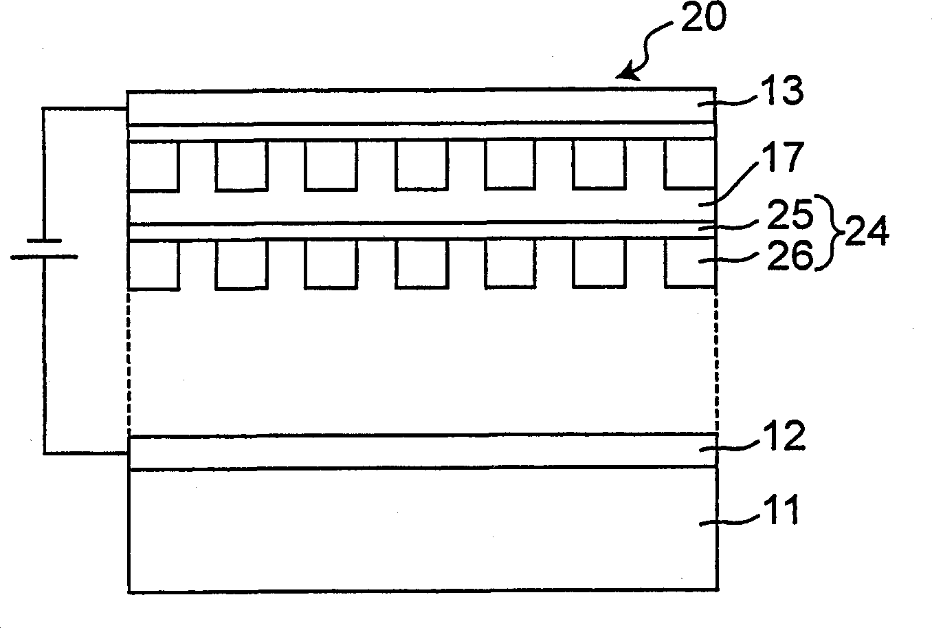
[0056] control figure 2 The related electroluminescent element 20 according to Embodiment 2 of the present invention will be described. This electroluminescent element 20 differs from the related electroluminescent element of Embodiment 1 in that the semiconductor layer 25 constituting the light emitting layer 24 with a large energy band gap is a continuous layer.

Embodiment approach 3

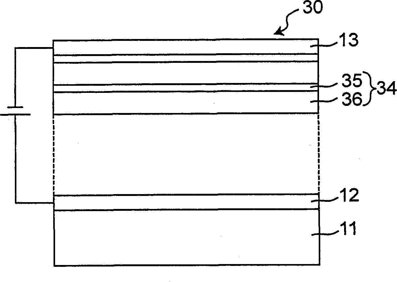
[0058] control image 3 The related electroluminescent element 30 according to Embodiment 3 of the present invention will be described. This electroluminescent element 30 differs from the related electroluminescent element of Embodiment 1 in that the semiconductor layer 35 and the phosphor layer 36 constituting the light emitting layer 34 with a large band gap are both continuous layers.


PUM


Abstract

An electroluminescent device (10) comprises a pair of anode (12) and cathode (13) arranged opposite to each other and one or more light-emitting layers (14) which are formed between the anode and the cathode. At least one of the light-emitting layers (14) is composed of a phosphor layer (16) and a wide band gap semiconductor layer (15). The semiconductor layer or the phosphor layer constituting the light-emitting layer may be a partially discontinuous layer.

Description

technical field [0001] The invention relates to a plane light source and an electric field luminescent element used in a plane display device. Background technique [0002] Conventional light-emitting devices used in planar light sources and planar display devices use light-emitting diodes, electroluminescent elements (called EL elements), and the like. [0003] Light-emitting diodes are excellent in that they have high luminance and high luminous efficiency, but they need to be formed on a compound semiconductor substrate, and it is difficult to increase the area of ​​one semiconductor substrate. In addition, in order to increase the size of the flat-panel display device, it is necessary to arrange a plurality of light-emitting diodes two-dimensionally. [0004] control Figure 5 The structure of the EL element will be described. Figure 5 This is a cross-sectional view illustrating the structure of an EL element. The EL element 50 has a unit structure in which a light-em...

Claims


Application Information

Patent Timeline
IPC IPC(8): H05B33/14C09K11/00C09K11/02C09K11/08
Inventor 名古久美男小田桐优小野雅行堀贤哉
Owner PANASONIC CORP
Why Eureka
Try Eureka