Apparatus and method for testing conductive bumps

A technology of conductive bumps and testing devices, which is used in measurement devices, semiconductor/solid-state device testing/measurement, and single semiconductor device testing, etc., can solve problems such as labor time-consuming, unsuitable for product wafer testing and evaluation, etc.

Active Publication Date: 2006-05-31
TAIWAN SEMICON MFG CO LTD
View PDF2 Cites 3 Cited by
  • Summary
  • Abstract
  • Description
  • Claims
  • Application Information

AI Technical Summary

Problems solved by technology

However, such existing daisy-ring detection methods require a lot of labor and are time-consuming
Furthermore, the above-mentioned daisy-ring detection method is only used for evaluating a bump process and its process parameters, and is not suitable for testing and evaluating product dies in today's integrated circuit industry.

Method used


Image

  • Apparatus and method for testing conductive bumps
  • Apparatus and method for testing conductive bumps
  • Apparatus and method for testing conductive bumps

Examples


Embodiment Construction

[0031] In order to make the above and other objects, features and advantages of the present invention more comprehensible, a preferred embodiment is specifically cited below, together with the accompanying drawings, and is described in detail as follows:

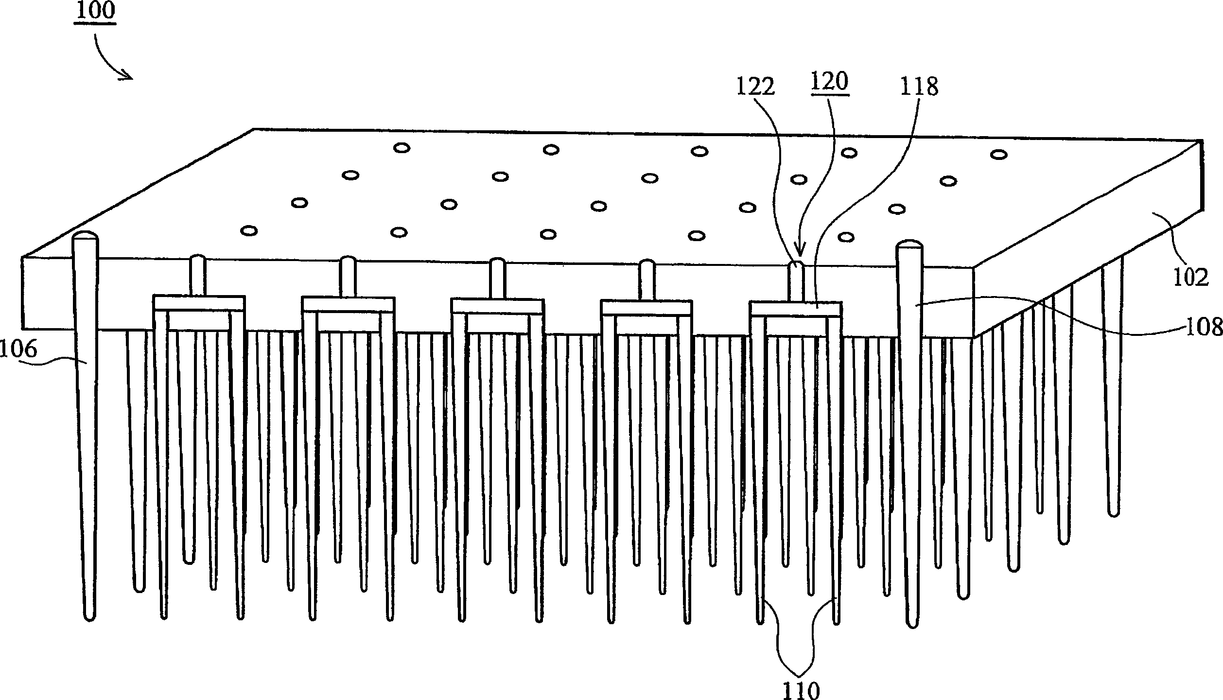
[0032] Embodiments of the invention will Figure 3 to Figure 7 Make a detailed description as follows. Figure 3 to Figure 6 is a series of schematic diagrams for illustrating a conductive bump testing device according to an embodiment of the present invention, and Figure 7 It is a flowchart for illustrating a conductive bump testing method according to an embodiment of the present invention.

[0033] Please refer to image 3 , illustrates an apparatus 100 for testing conductive bumps. Here, the device 100 includes a support substrate 102 in which a plurality of test probes are formed. The support substrate 102 includes an insulating material such as ceramic material, epoxy, resin, polyimide, FR4 glass fiber, or polymer...


PUM


Abstract

The present invention relates to a conductive bump testing device and a testing method. The conductive bump testing device is suitable for testing a plurality of conductive bumps, including: a supporting substrate; The probe, a second probe, and a plurality of dual probe sets, wherein each dual probe set includes two third probes electrically connected. The conductive bump testing device and testing method described in the present invention can be applied immediately after the bump is formed, so as to check the quality of the formed bump and the applied bump process in real time.

Description

technical field [0001] The present invention relates to wafer-level bumps testing related technologies, and in particular to a testing device and testing method for testing conductive bumps on semiconductor components. Background technique [0002] Flip-chip packaging of electronic products is to directly electrically connect electronic components to a substrate, such as a ceramic substrate, a circuit board, or a substrate using a conductive bump pad carrier, with the active surface facing down. Flip-chip technology has rapidly replaced the traditional wire-bonding technology that uses wires to connect the active in-plane pads with the die facing up. [0003] Flip-chip packaging technology is usually achieved by placing solder bumps on a silicon wafer. The solder bump flip-chip process usually includes four consecutive process steps, including: (1) preparing a wafer for solder bumping; (2) forming and placing solder bumps on the wafer; (3) placing the wafer The chip with s...

Claims


Application Information

Patent Timeline
Patent Type & Authority Applications(China)
IPC IPC(8): H01L21/66G01R31/26
CPCG01R1/06794G01R1/07307
Inventor 郭彦良
Owner TAIWAN SEMICON MFG CO LTD
Why Eureka
Try Eureka