Copper interconnect structure with modulated topography and method for forming the same

A technology of wire structure and copper interconnection, applied in semiconductor/solid-state device manufacturing, electrical components, circuits, etc., can solve the problems of general product lack and inconvenience, and achieve the effect of solving electronic drift and stress drift

Inactive Publication Date: 2006-04-26
TAIWAN SEMICON MFG CO LTD
View PDF0 Cites 5 Cited by
  • Summary
  • Abstract
  • Description
  • Claims
  • Application Information

AI Technical Summary

Problems solved by technology

[0004] It can be seen that the above-mentioned existing copper interconnection structure and the method for manufacturing the copper interconnection structure obviously still have inconvenience and defects in structure, method and use, and need to be further improved urgently
In order to solve the problems existing in the copper interconnection structure and the method of manufacturing the copper interconnection structure, the relevant manufacturers have tried their best to find a solution, but no suitable design has been developed for a long time, and general products have not been developed. Appropriate structures can solve the above problems, which is clearly a problem that relevant industry players are eager to solve

Method used


Image

  • Copper interconnect structure with modulated topography and method for forming the same
  • Copper interconnect structure with modulated topography and method for forming the same
  • Copper interconnect structure with modulated topography and method for forming the same

Examples


Embodiment Construction

[0052] In order to further illustrate the technical means and effects that the present invention adopts to achieve the intended purpose of the invention, below in conjunction with the accompanying drawings and preferred embodiments, the copper interconnection structure with improved configuration proposed according to the present invention and the manufacture of the interconnection The specific implementation, structure, method, steps, features and effects of the wire structure method are described in detail below.

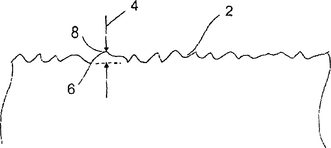
[0053] An embodiment of the present invention provides an adjustment structure to improve the reliability of copper interconnects in semiconductor devices. The adjustment structure includes forming rough or wavy topography on the surface of copper interconnect bonding pads. The rough or wavy configuration is used to slow down the drift speed of copper metal, so as to eliminate the effect of electron drift and stress drift, so that the improvement factor of reliabil...


PUM

PropertyMeasurementUnit
surface roughnessaaaaaaaaaa

Abstract

The present invention relates to a copper interconnection structure of a semiconductor device. The roughness of the surface area of ​​the structure is greater than 20 angstroms, preferably greater than 100 angstroms. The surface area of ​​the copper interconnection structure is in contact with another rough surface formed by ion bombardment to solve the problems of electron drift and stress drift in the copper interconnection structure.

Description

technical field [0001] The present invention relates to a semiconductor element and its manufacturing method, and in particular to a copper interconnection structure and a method for manufacturing the interconnection structure. Background technique [0002] Since copper metal has high-speed signal transmission characteristics, it is often used as a material for conductive interconnects of semiconductor devices. When a damascene process is used to form copper interconnect bond pads, an opening is formed in a dielectric layer, and copper metal is deposited in the opening, followed by a grinding / planarization process step to remove excess on the dielectric layer. The copper metal material, so that the copper metal is embedded in the opening. Therefore, the copper interconnect bond pads can be in contact with the sidewalls and bottom surfaces of the openings. Traditionally, the openings are formed by plasma etching, and the sidewalls and bottom surfaces of the openings are ver...

Claims


Application Information

Patent Timeline
Patent Type & Authority Applications(China)
IPC IPC(8): H01L21/3205H01L21/52H01L21/768
CPCH01L21/76825H01L21/76814
Inventor 范淑贞陈学忠
Owner TAIWAN SEMICON MFG CO LTD
Why Eureka
Try Eureka