Substrate processing apparatus and substrate positioning device

A substrate processing device and a technology for substrates, which can be applied to devices that apply liquid to surfaces, machines that arrange working positions in sequence, and coating of discharge tubes, etc. , to achieve the effect of saving space

Active Publication Date: 2006-03-15
TOKYO ELECTRON LTD
View PDF1 Cites 32 Cited by
  • Summary
  • Abstract
  • Description
  • Claims
  • Application Information

AI Technical Summary

Problems solved by technology

However, it is difficult to apply this conventional substrate positioning device to a spinless resist coating device.
That is, the linear push mechanism requires a considerable amount of dedicated space, resulting in an increase in size and complexity around the stage, and unavoidable interference with the scanning mechanism for the elongated resist nozzle.

Method used


Image

  • Substrate processing apparatus and substrate positioning device
  • Substrate processing apparatus and substrate positioning device
  • Substrate processing apparatus and substrate positioning device

Examples


Embodiment Construction

[0051] Below, we refer to the attached Figure 1 Preferred embodiments of the present invention will be described above.

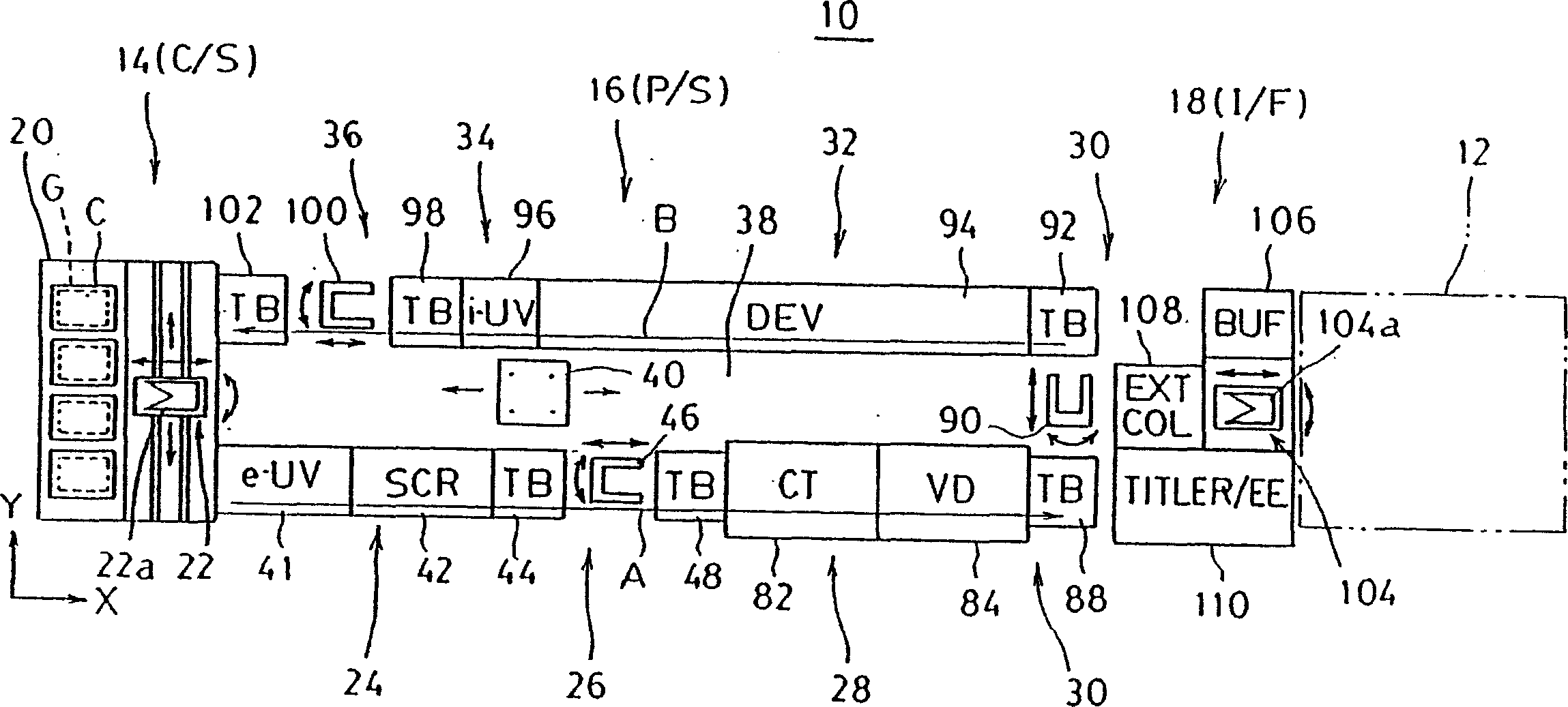
[0052] figure 1 A coating and development processing system is shown as an example of the configuration of a substrate processing apparatus to which the present invention can be applied. The coating and development processing system 10 is set in a clean room, for example, the LCD substrate is used as the substrate to be processed, and the cleaning, resist coating, pre-baking, development and post-processing in the photolithography process are performed in the LCD manufacturing process. A series of processes such as baking. Exposure processing is performed by an external exposure device 12 provided adjacent to the processing system.

[0053] In this coating and development processing system 10, a horizontally long processing station (P / S) 16 is arranged at the central part, and a cartridge mounting station (C / S) 14 and an interface station are arranged a...


PUM


Abstract

PROBLEM TO BE SOLVED: To position a substrate to be processed efficiently by saving space. ŽSOLUTION: After having transferred a substrate G to a lift pin 132, each rotation driving portion 152 rotates each eccentric movable alignment pin 150 to nearly half rotating location from an original location through a rotation driving shaft 154. Then, the alignment pin 150 transfers toward each side of the substrate G in face to face with the pin while performing eccentric rotating movement, and a collar (contacting portion) 150b contacts with a substrate edge (substrate side). Furthermore, the pin pushes the substrate G from there. This makes the substrate G in displacement or transfer toward a pushed direction on the lift pin 132, and the opposite long side of the substrate G is pushed to a fixing alignment pin. As a result, the substrate G is caught in between the eccentric movable alignment pin 150 and the fixing alignment pin, then its positioning is finished. Ž

Description

technical field [0001] The present invention generally relates to a substrate processing apparatus that applies processing to a substrate to be processed on a stage, and particularly relates to a technique for determining a position of a substrate. Background technique [0002] Recently, in the photolithography process of the flat panel display (FPD) manufacturing process, as a resist coating method that is advantageous for increasing the size of the substrate to be processed (such as a glass substrate), the substrate is sprayed with a resist nozzle A non-spin method that sprays resist solution with a fine diameter continuously, and applies a resist solution with a desired film thickness on the substrate without rotational motion by relatively moving the resist nozzle while scanning is becoming popular. [0003] Generally, according to the resist coating apparatus of the non-spin system, as described in Patent Document 1, for example, a substrate placed horizontally on a sta...

Claims


Application Information

Patent Timeline
IPC IPC(8): G03F9/00G03F7/16B05C5/02H01L21/027H01L21/68
CPCG03F7/707H01J9/20H01J9/48H01J2209/015H01L21/027H01L21/68
Inventor 元田公男立山清久富田龙生
Owner TOKYO ELECTRON LTD
Why Eureka
Try Eureka