
Color filter imaging array and method of formation

A color filter array and color filter technology, applied in the field of color filters, can solve problems such as low spectral reflectance

Inactive Publication Date: 2005-09-14
APTINA IMAGING CORP
View PDF6 Cites 94 Cited by
  • Summary
  • Abstract
  • Description
  • Claims
  • Application Information

AI Technical Summary

Problems solved by technology

However, if the object being imaged has relatively low spectral reflectance at wavelengths in the green portion, the image captured using an imager with a Bayer filter pattern may not be optimal

Method used


Image

  • Color filter imaging array and method of formation
  • Color filter imaging array and method of formation
  • Color filter imaging array and method of formation

Examples


Embodiment Construction

[0022] The present invention will be described in detail below with reference to the accompanying drawings, which form a part of the present invention and in which specific embodiments in which the present invention can be practiced are described by way of illustration. These embodiments are described in sufficient detail to enable those skilled in the art to practice the invention, it being understood that other embodiments may be utilized and that structural, logical and electronic modifications may be made without departing from the spirit and scope of the invention. make change.

[0023] The terms "wafer" and "substrate" shall be understood to include silicon-on-insulator (SOI) or silicon-sapphire (SOS) technology, doped or undoped semiconductors, silicon epitaxial layers supported by semiconductor substrates, and other semiconductor structures . Also, when referring to a "wafer" or "substrate" in the following description, preceding processing steps may be utilized to fo...


PUM


Abstract

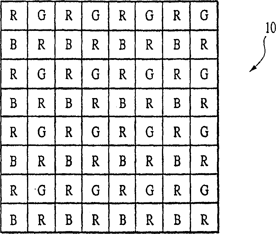
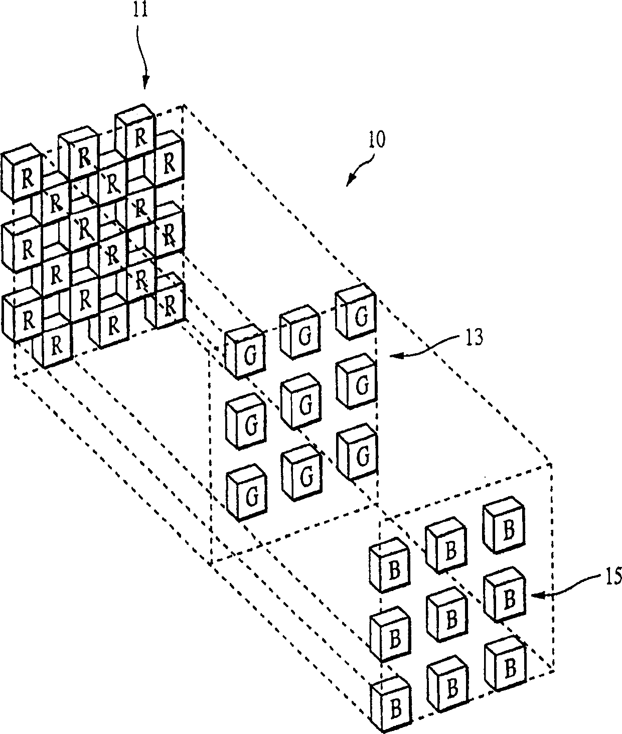
A color filter array pattern for use in a solid-state imager comprising red sensitive elements located at every other array position, with alternating blue sensitive and green sensitive elements located at the remaining array positions, is disclosed. Since red color is sampled most frequently, the color filter may be part of an in vivo camera system for imaging internal human body organs and tissues.

Description

technical field [0001] The present invention relates to a color filter for use in a solid-state image sensor, and in particular to a patterned color filter array that samples red more frequently than blue and green, and a method of forming it. Background technique [0002] Solid-state image sensors, also known as imagers, were developed in the late 1960s and early 1970s, mainly for television image acquisition, transmission and display. Imagers absorb incident radiation of a particular wavelength (such as photons, x-rays, etc.) and generate electrical signals corresponding to the absorbed radiation. There are many different types of semiconductor-based imagers, including charge coupled devices (CCDs), photodiode arrays, charge injection devices (CIDs), hybrid focal plane arrays, and CMOS imagers. Current applications for solid state imagers include cameras, scanners, machine vision systems, vehicle navigation systems, video telephony, computer input devices, surveillance sy...

Claims


Application Information

Patent Timeline
IPC IPC(8): G02B5/20A61B1/04H01L27/14H01L27/146H04N5/335H04N9/04H04N9/07
CPCH01L27/14603H01L27/14609H01L27/14621H01L27/14627H01L27/14643H04N9/045Y10S600/921H04N25/134G02B5/20H04N23/10
Inventor K·文卡塔拉曼
Owner APTINA IMAGING CORP
Learn More