


Quick Research
Generate reliable direction feasibility study reports for your R&D in just a few steps.

Technical Q&A
Discover and master advanced knowledge NOW. Basics, ideas, possibilities, all at once.

Find Solutions
As an expert in R&D theories, this can generate solutions to your technical problems instantly.

Evaluate Feasibility
Analyze your overall solution with one click, know your potential R&D risks in advance.

Monitor Landscape
Get weekly tech updates, stay abreast of the latest tech innovations and key insights.
Laser irradiation apparatus, laser irradiation method, and method for manufacturing crystalline semiconductor film
A technology of laser irradiation and manufacturing method, which is applied in the manufacture of semiconductor/solid-state devices, lighting devices, semiconductor devices, etc. question
- Summary
- Abstract
- Description
- Claims
- Application Information
AI Technical Summary
Problems solved by technology
Method used
Image

Examples
Embodiment 1
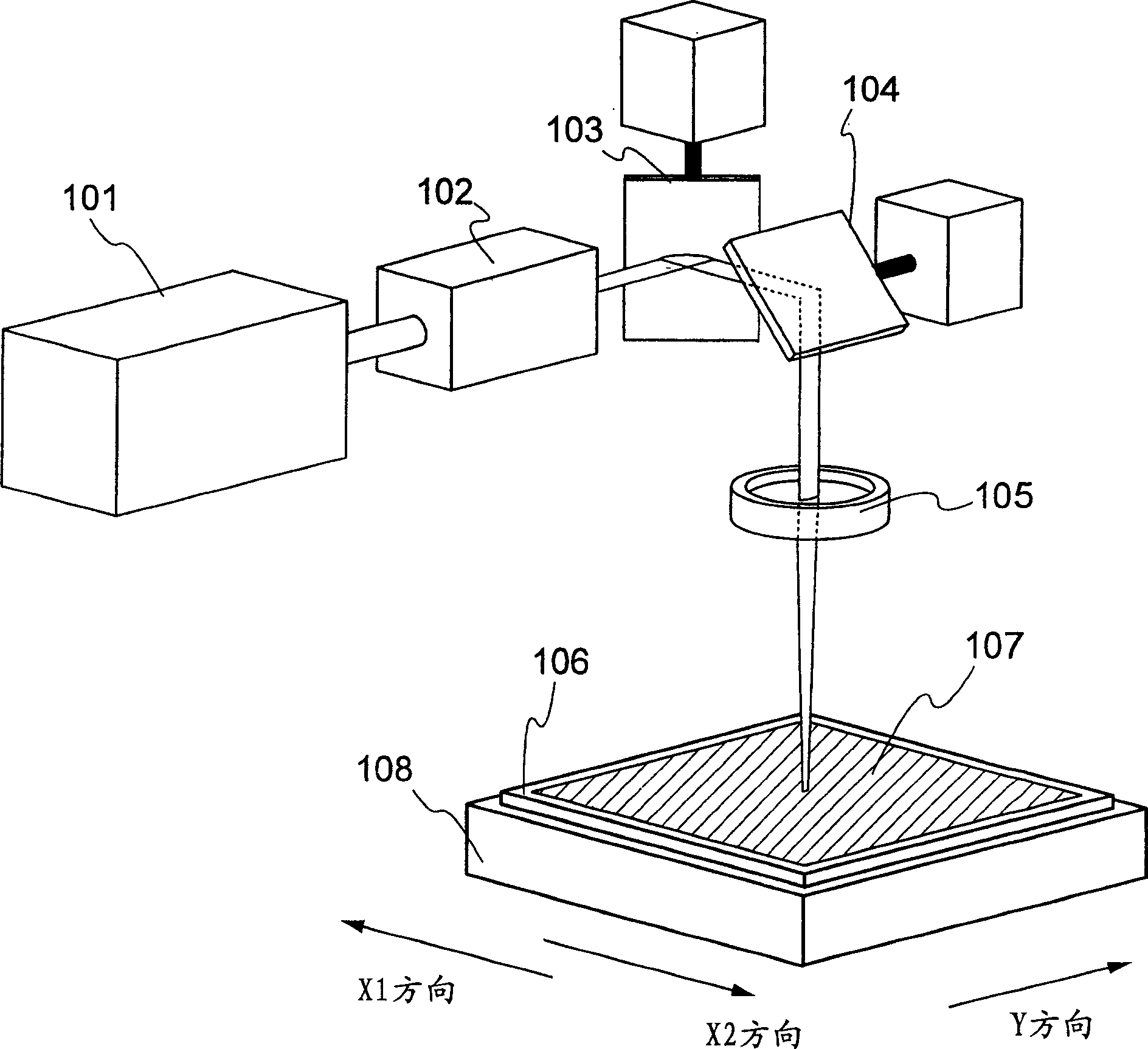
[0157] This example will refer to figure 1 Examples of the present invention will be described.
[0158] 101 denotes a laser oscillator for pulse oscillation, which is a laser oscillator capable of oscillating laser light with a pulse width of picosecond level or less. Any laser can be used for the laser oscillator of the present invention as long as it can oscillate an extremely short-pulse laser beam of 10 psec or less. For example, excimer lasers, Ar lasers, Kr lasers, CO 2 Laser, YAG laser, Y 2 o 3 Laser, YVO 4 Laser, YLF laser, YAlO 3 Laser, GdVo 4 Lasers, ceramic lasers, glass lasers, ruby lasers, alexandrite lasers, Ti:sapphire lasers, copper vapor lasers, or gold vapor lasers, etc.
[0159] This example uses 2W YVO 4 laser. The laser oscillator incorporates a nonlinear optical element, and emits laser light with a wavelength of 532nm at the second harmonic of the laser light, which has a high absorption rate for the amorphous silicon film. It is desirable t...
Embodiment 2
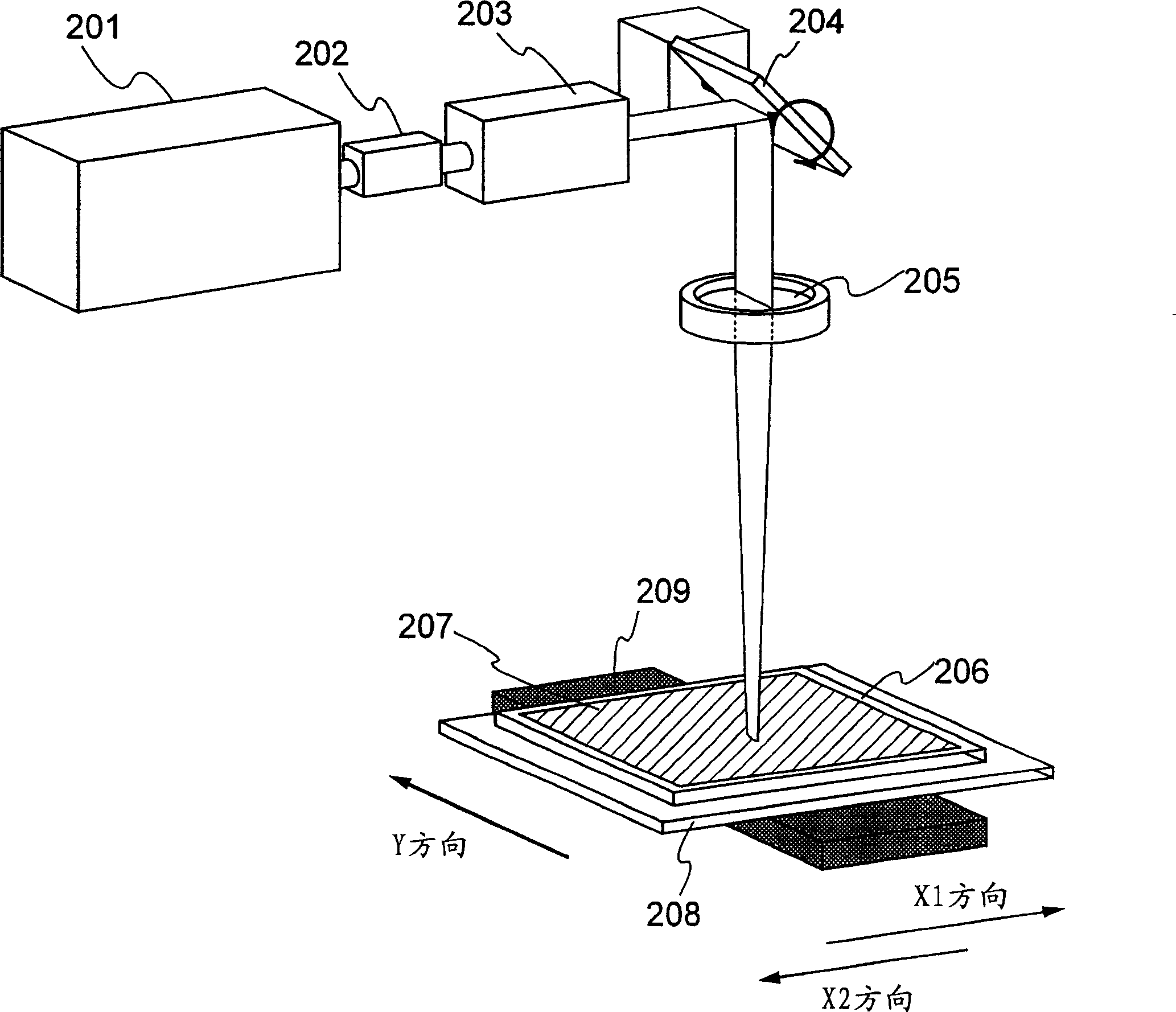
[0174] This example will refer to image 3 An example of a laser irradiation device including a laser oscillator 201 that oscillates laser light with a pulse width of picosecond level or below; an electric mirror 204 driven in one direction; an fθ lens 205 is described. ; The stage 208 and the mobile robot 209 moving in one direction.
[0175] A laser beam output from a laser oscillator 201 is converted into a second harmonic wave by a nonlinear optical element 202 and shaped into an arbitrary shape by an optical system 203 . In this embodiment, the configuration of the optical system 203 is such that the shape of the beam spot on the irradiation surface is formed into a line shape. Thereafter, the semiconductor film 207 formed on the glass substrate 206 is scanned with a linear laser beam (X1 direction) using the galvanic mirror 204 and the fθ lens 205 . Note that, in the case of using a linear beam, laser irradiation can be efficiently performed if the minor axis direction...
Embodiment 3
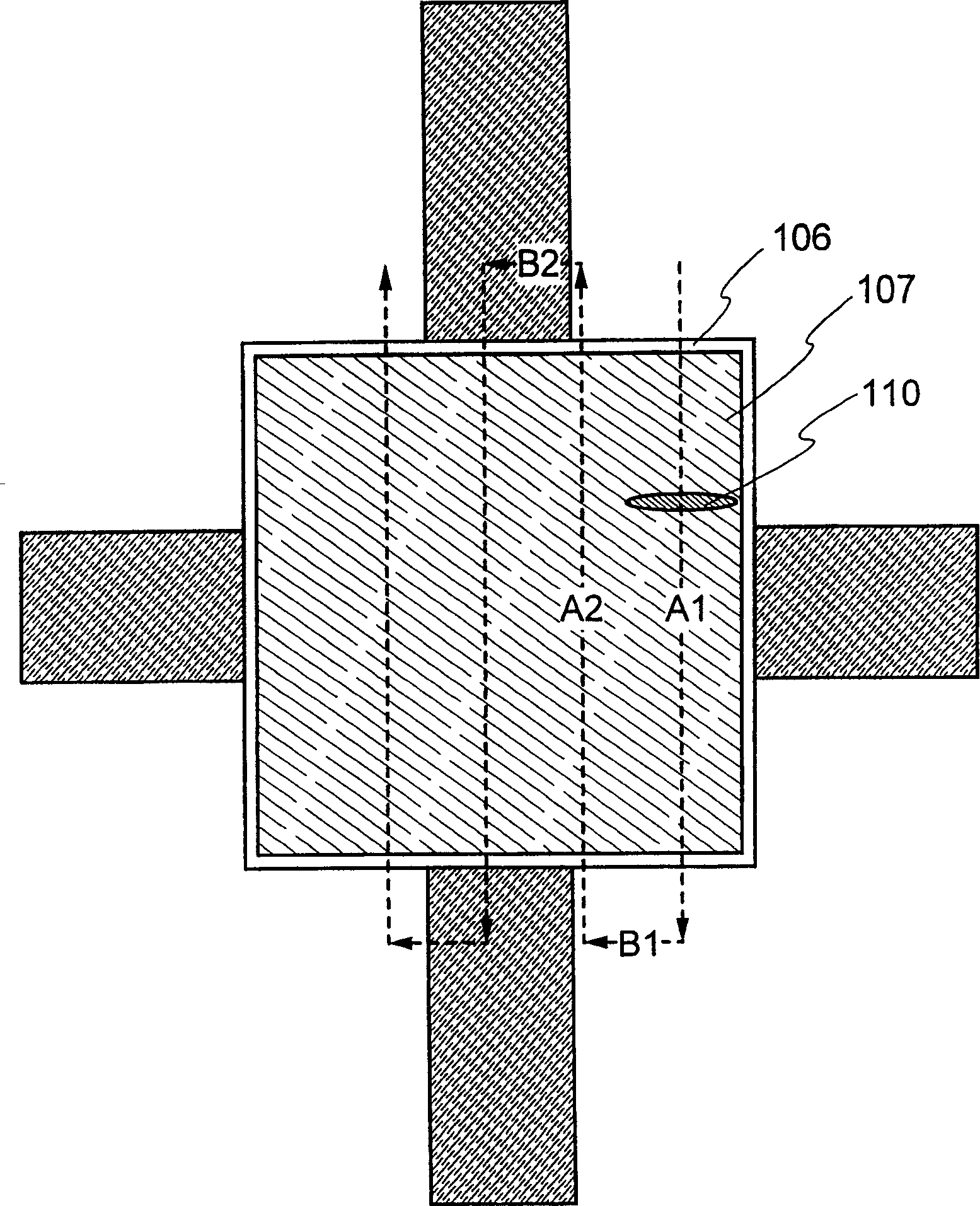
[0180] This example will refer to Figure 4 Another embodiment mode of the present invention will be described. In this embodiment, an example will be described in which laser crystallization is performed only on a position where a TFT is formed in an amorphous semiconductor film formed on a substrate.
[0181] The laser oscillator 401 is a laser oscillator capable of oscillating a laser beam of an extremely short pulse at or below the picosecond level. A laser beam with a pulse width of 10 psec, a wavelength of 532 nm, an output power source of 8 W, a repetition frequency of 80 MHz, and a beam diameter of 0.6 mm was oscillated from this oscillator. The oscillated laser beam is shaped into an arbitrary shape by the optical system 402 . In this embodiment, the beam shape on the semiconductor film 408 formed on the substrate 407 on the irradiation surface is shaped by using a lenticular lens acting only in the uniaxial direction so that the beam shape becomes 300 μm in the maj...
PUM
| Property | Measurement | Unit |
|---|---|---|
| frequency | aaaaa | aaaaa |
| width | aaaaa | aaaaa |
| thickness | aaaaa | aaaaa |
Abstract
Description
Claims
Application Information
 - R&D Engineer
- R&D Manager
- IP Professional
- Industry Leading Data Capabilities
- Powerful AI technology
- Patent DNA Extraction
Browse by: Latest US Patents, China's latest patents, Technical Efficacy Thesaurus, Application Domain, Technology Topic, Popular Technical Reports.
© 2024 PatSnap. All rights reserved.Legal|Privacy policy|Modern Slavery Act Transparency Statement|Sitemap|About US| Contact US: help@patsnap.com