Photovoltaic apparatus
A technology for optoelectronic devices and photoelectric conversion layers, which can be used in photovoltaic power generation, circuits, electrical components, etc., and can solve problems such as difficulty in light trapping effect, difficulty in output characteristics, and difficulty in light scattering.
- Summary
- Abstract
- Description
- Claims
- Application Information
AI Technical Summary
Problems solved by technology
Method used
Image


Examples
Embodiment 1
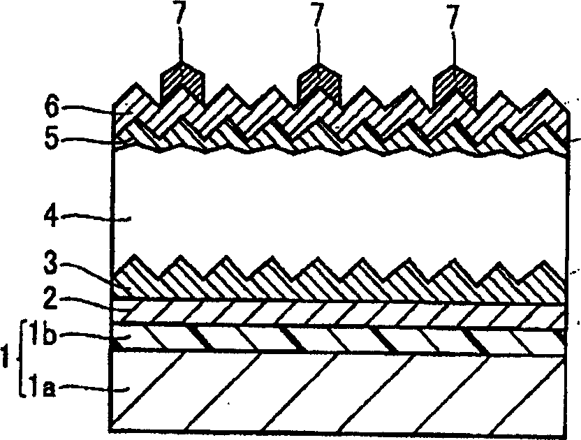
[0049] refer to figure 1 , First, the structure of the photovoltaic device according to Embodiment 1 of the present invention will be described.
[0050] In the photovoltaic device according to Embodiment 1, such as figure 1 As shown in , on a flat stainless steel plate (SUS430) 1 a having a thickness of 0.15 mm, a polyimide resin 1 b having a thickness of 20 μm was formed. The substrate 1 is formed by this stainless steel plate 1a and polyimide resin 1b. On the substrate 1 (polyimide resin 1b), a flat back electrode 2 composed of Ag (silver) having a thickness of 200 nm was formed.
[0051] On the back electrode 2, an n-type layer 3 composed of an n-type microcrystalline silicon layer having a thickness of 50 nm was formed. On n-type layer 3 , photoelectric conversion layer 4 composed of an undoped microcrystalline silicon layer having a thickness of 2 μm is formed. A p-type layer 5 composed of a p-type microcrystalline silicon layer having a thickness of 20 nm is formed ...
Embodiment 2
[0069] refer to image 3 , First, the structure of the photovoltaic device according to Example 2 fabricated according to the present invention will be described.
[0070] In the photovoltaic device according to the present embodiment 2, such as image 3 As shown in FIG. 1 , the rear electrode 2 is formed on the substrate 1 composed of the stainless steel plate 1 a and the polyimide resin 1 b in the same manner as in the first embodiment. On the back electrode 2, an n-type layer 13 composed of an n-type microcrystalline silicon layer having a thickness of 50 nm was formed. On n-type layer 13 , photoelectric conversion layer 14 composed of an undoped microcrystalline silicon layer having a thickness of 2 μm is formed. A p-type layer 15 composed of a p-type microcrystalline silicon layer having a thickness of 20 nm was formed on the photoelectric conversion layer 14 . Furthermore, a power generating unit is constituted by the n-type layer 13 , the photoelectric conversion lay...
Embodiment 3
[0086] refer to Figure 5 , in this embodiment 3, different from the above-mentioned embodiments 1 and 2, the n-type layer is formed to have a preferential crystal orientation of the (111) plane, and the photoelectric conversion layer and the p-type layer are formed to have the (220) plane Examples of preferred crystallographic orientations are described.
[0087] In the photoelectric device according to the present embodiment 3, such as Figure 5 As shown in FIG. 1 , the rear electrode 2 is formed on the substrate 1 composed of the stainless steel plate 1 a and the polyimide resin 1 b in the same manner as in the first embodiment. On the back electrode 2, an n-type layer 43 composed of an n-type microcrystalline silicon layer having a thickness of 50 nm was formed. On the n-type layer 43 , a photoelectric conversion layer 44 composed of an undoped microcrystalline silicon layer having a thickness of 2 μm is formed. A p-type layer 45 composed of a p-type microcrystalline si...
PUM
 Abstract
Description
Claims
Application Information
 - Generate Ideas
- Intellectual Property
- Life Sciences
- Materials
- Tech Scout
- Unparalleled Data Quality
- Higher Quality Content
- 60% Fewer Hallucinations
Browse by: Latest US Patents, China's latest patents, Technical Efficacy Thesaurus, Application Domain, Technology Topic, Popular Technical Reports.
© 2025 PatSnap. All rights reserved.Legal|Privacy policy|Modern Slavery Act Transparency Statement|Sitemap|About US| Contact US: help@patsnap.com