High-frequency throwing structure

A wire structure, high-frequency technology, applied in the direction of electrical components, electrical solid devices, circuits, etc., can solve problems such as difficulty in implementation, counter-effects, contact between two dozen wires, etc., to achieve the best electrical characteristics, best capacitance and inductance matching, avoid The effect of too close between lines

Active Publication Date: 2005-03-16
VIA TECH INC
View PDF0 Cites 1 Cited by
  • Summary
  • Abstract
  • Description
  • Claims
  • Application Information

AI Technical Summary

Problems solved by technology

[0008] However, such an improvement of the high-frequency wire bonding structure 100 is difficult to implement.
For example, the bonding area between the bonding pad 133 and the pin 140 is actually not large, so the two bonding wires between the bonding pad 133 and the pin 140 must be very close, and it is difficult to implement when bonding. In the future, when the adhesive film is applied, the adhesive film will easily make two dozen wires contact and produce adverse effects

Method used


Image

  • High-frequency throwing structure
  • High-frequency throwing structure
  • High-frequency throwing structure

Examples


Embodiment Construction

[0040] In order to make the characteristics, purpose and functions of the present invention be further recognized and understood, the detailed description is as follows in conjunction with the accompanying drawings:

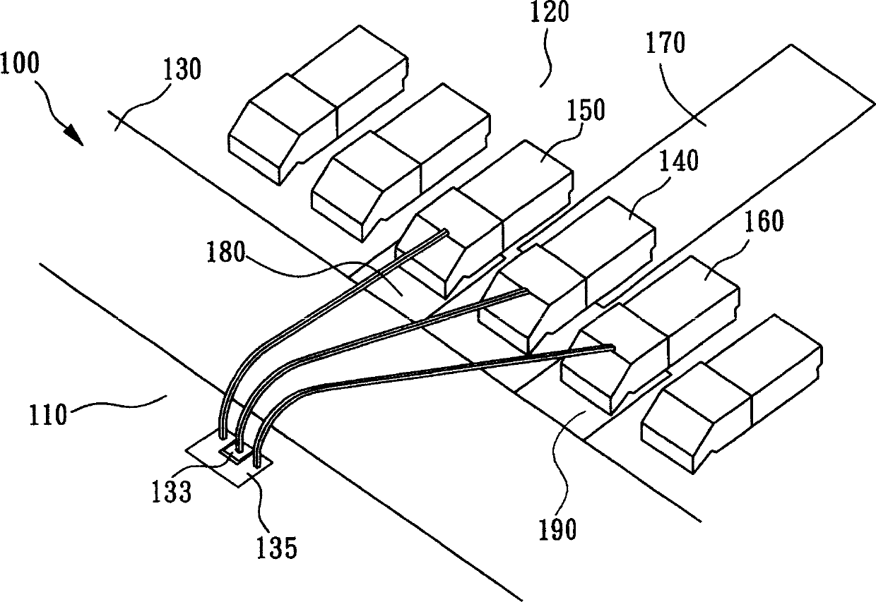
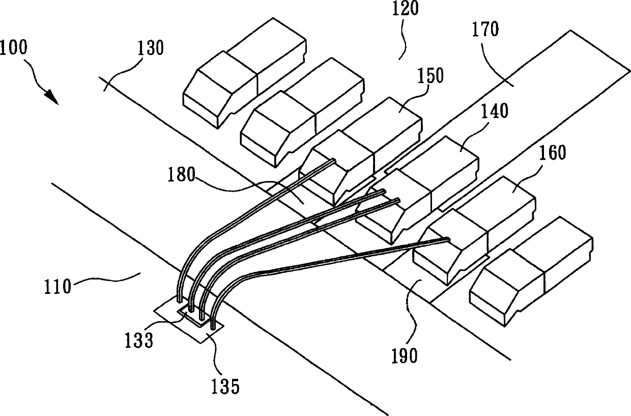
[0041] The present invention is based on the high-frequency bonding structure generally used in radio frequency or high-speed circuits. In order to make the electrical characteristics between the chip and the package better, the signals are usually output in parallel, and the two adjacent sides of the signals are respectively Ground loop, so the bonding between the chip and the package is very dense. Therefore, it is difficult to implement wire bonding, and it is easy to cause contact between wires in the future when the adhesive film is applied, thereby greatly reducing the electrical characteristics between the chip and the package.

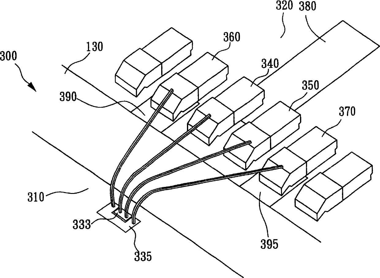
[0042] Therefore, the present invention considers that in addition to outputting the high-frequency signal bonding pads at the c...


PUM


Abstract

Disclosed is a high frequency throwing structure, mainly comprising multi-throwing pads on the end chip with multi-throwing pads and multi-throwing pads on the end of seal agent. Its characteristics is that, the connecting type of high efficiency signal is on multi-throwing pads on the end of chip has the output two near adjacent multi-throwing pads to the seal agent in parallel method, and the connecting type of earthling signal is high frequency signal which has two earthling loop nearby, especially a multi-throwing pads on the end of seal agent is shared by two adjacent multi-throwing pads for output of high frequency signal. So the invention can avoiding too fewer distance between throwing, and can acquire good match of capacitance and inductance each other between chip and with good electric specification.

Description

technical field [0001] The invention relates to a high-frequency wire bonding structure, in particular to a high-frequency wire bonding structure used in metal frame packaging or lead frame packaging. Background technique [0002] In radio frequency circuits or high-speed circuits, in the high-frequency bonding structure, although the high-frequency signal bonding pads are often surrounded by grounding signal bonding pads on both sides of the chip end, and multi-point grounding is provided on the package, so that The electrical characteristics between the chip and the package can be better. But in this case, there are dense distribution of metal wires in the narrow space of the high-frequency wire bonding structure, so when the metal wires are wire-bonded, there will be troubles in the wire spacing, wire arc height, and wire layout. [0003] And when the high-frequency wire-bonding structure puts an adhesive film on the package to cover the chip and the metal wires, too den...

Claims


Application Information

Patent Timeline
IPC IPC(8): H01L23/28H01L23/48
CPCH01L2224/04042H01L2224/05553H01L2224/48257H01L2224/48247H01L24/06H01L2224/0603H01L24/05H01L2224/49171H01L2924/181H01L2924/00H01L2924/00012
Inventor 李胜源
Owner VIA TECH INC
Why Eureka
Try Eureka