Manufacturing a solar cell with backside contacts
A solar cell and backside technology, which is applied in the direction of final product manufacturing, sustainable manufacturing/processing, circuits, etc., can solve the problems of complex solar cells and cost hindering the large-scale application of solar cells, and achieve the effect of reliable regeneration
- Summary
- Abstract
- Description
- Claims
- Application Information
AI Technical Summary
Problems solved by technology
Method used
Image
Examples
Embodiment Construction
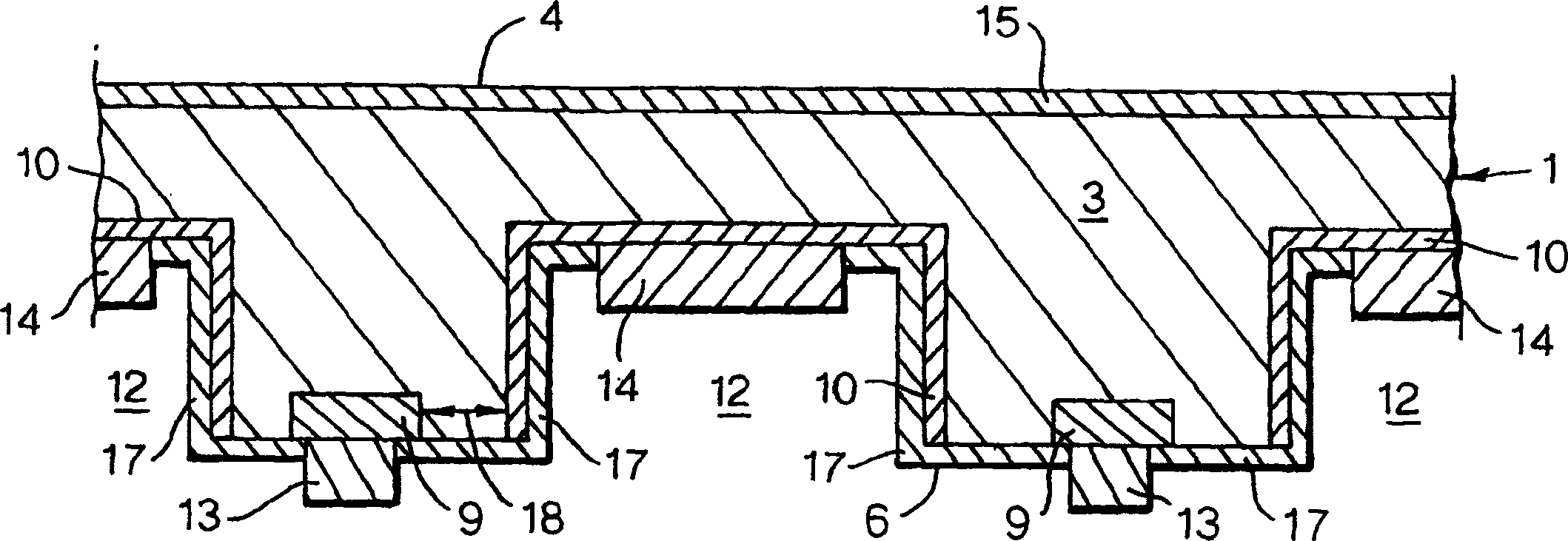
[0023] now refer to figure 1 , figure 1 A partial sectional view of a solar cell 1 according to the invention is shown schematically and not to scale.
[0024] The solar cell 1 comprises a silicon wafer 3 with a light-receiving front side 4 and a back side 6 . The silicon wafer 3 has a basic doping, in this example p-type doping.
[0025] On the back side 6, the silicon wafer 3 is provided with an interdigitated semiconductor pattern comprising at least one first pattern of first diffusion regions 9 with a first doping and at least one second diffusion region 10 of second pattern. The second diffusion region 10 is separated from the first diffusion region 9 and they have a second doping different from the first doping. Each second diffusion region 10 is arranged along the side of at least one trench 12 extending from the backside 6 into the silicon wafer 3 . A suitable number of grooves ranges from 1 to 100 grooves per centimeter of wafer width, suitable groove widths ran...
PUM
 Abstract
Description
Claims
Application Information
 - R&D
- Intellectual Property
- Life Sciences
- Materials
- Tech Scout
- Unparalleled Data Quality
- Higher Quality Content
- 60% Fewer Hallucinations
Browse by: Latest US Patents, China's latest patents, Technical Efficacy Thesaurus, Application Domain, Technology Topic, Popular Technical Reports.
© 2025 PatSnap. All rights reserved.Legal|Privacy policy|Modern Slavery Act Transparency Statement|Sitemap|About US| Contact US: help@patsnap.com


