Image sensor

An image sensor and sensor technology, applied in image communication, electrical solid-state devices, semiconductor devices, etc., can solve problems such as difficult to decompose

Inactive Publication Date: 2005-02-02
SII SEMICONDUCTOR CORP
View PDF1 Cites 10 Cited by
  • Summary
  • Abstract
  • Description
  • Claims
  • Application Information

AI Technical Summary

Problems solved by technology

Also, since the dummy pixels in the conventional image sensor IC are provided separately from the light-receiving device, which means that different common signal lines and different pixels are used, due to differences in wiring capacitance levels between the common signal lines, by Fixed pattern noise, switching noise, and temperature characteristics inherent in each IC due to voltage drop due to power line point resistance that only long ICs have, making it difficult to match dark levels while decomposing factors under unbalance

Method used


Image

  • Image sensor
  • Image sensor
  • Image sensor

Examples


Embodiment Construction

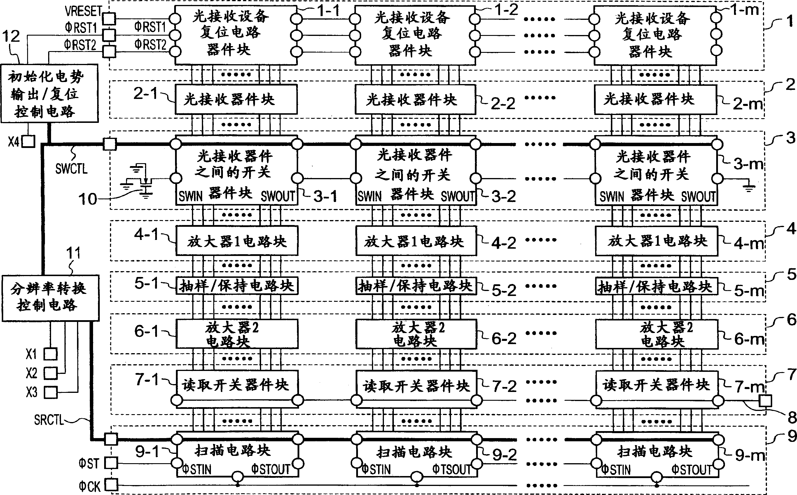
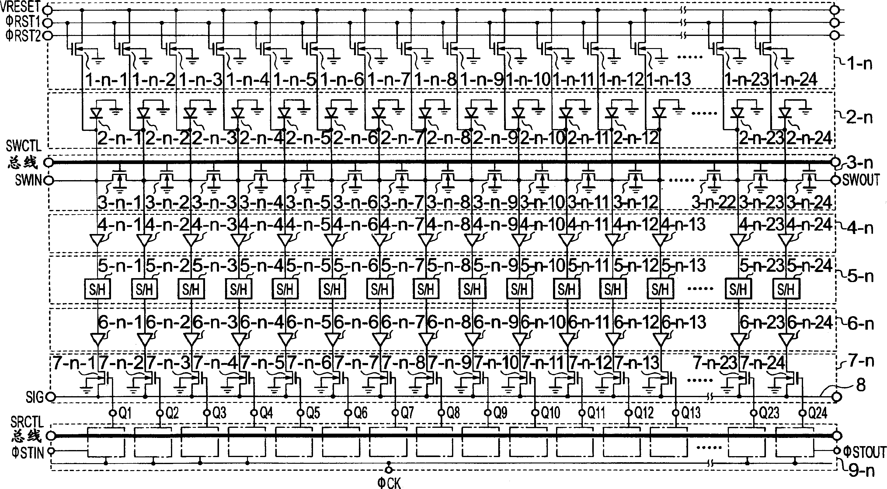
[0030] Embodiments of the present invention will be described below with reference to the drawings. figure 1 is a general circuit diagram of an image sensor according to an embodiment of the present invention. figure 2 yes figure 1 The circuit diagram of the nth module in . Figure 21 shown in figure 2 Setting of switches 3-n-1, -2, -3, . . . -24 among the light receiving devices. Figure 22 shown in figure 2 Setup for testing of switches 3-n-1, -2, -3, . . . -24 among light-receiving devices.

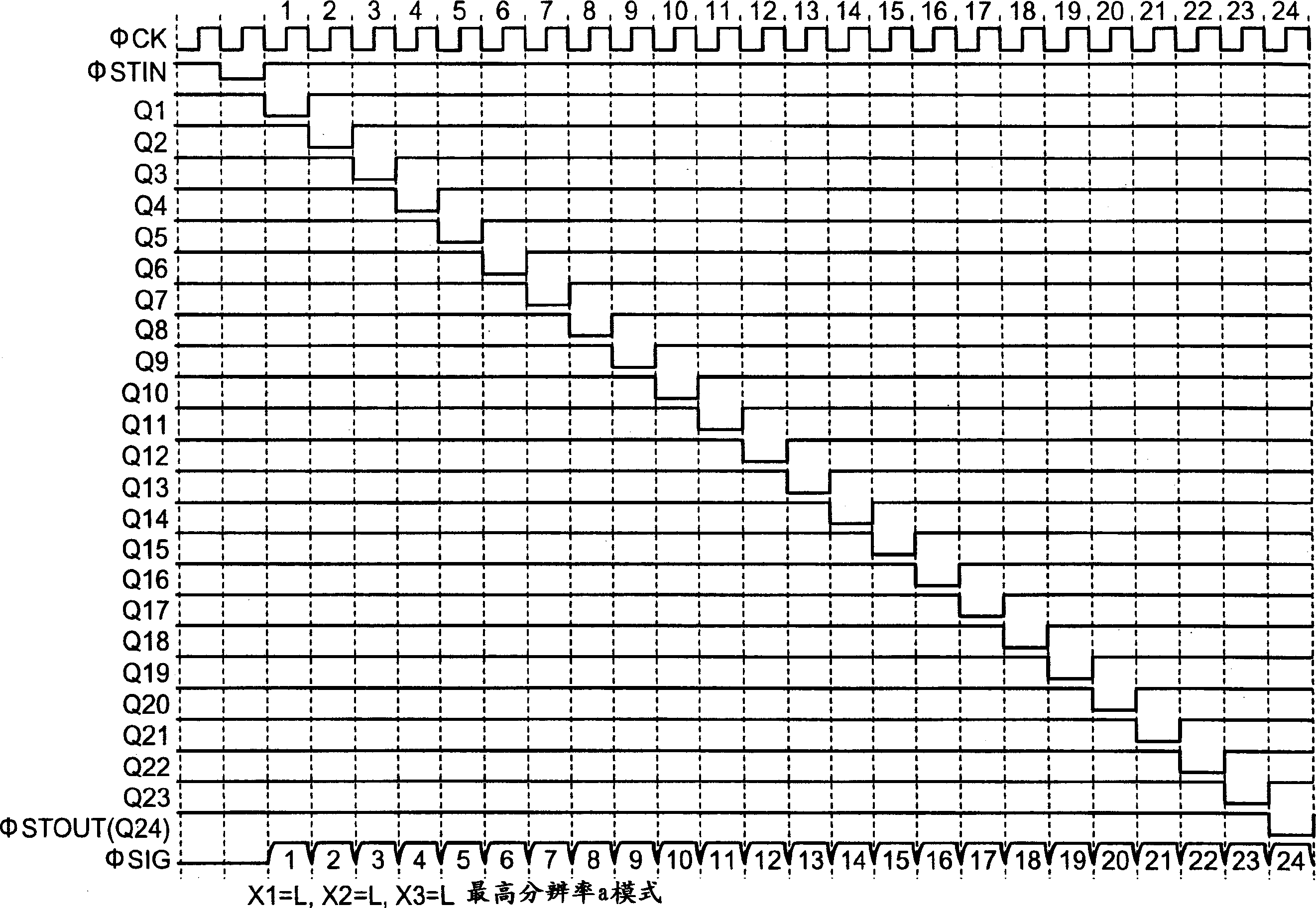
[0031] image 3 is a timing chart when the resolution is the highest resolution a. Figure 4 is a timing chart when the resolution is the highest resolution a×1 / 2. Figure 5 is a timing chart when the resolution is the highest resolution a×1 / 4.

[0032] Figure 6 is a timing chart when the resolution is the highest resolution a×1 / 6. Figure 7 is a timing chart when the resolution is the highest resolution a×1 / 8. Figure 8 is the timing diagram of TEST1 mode. Figure 9 It...


PUM


Abstract

An image sensor capable of arbitrarily outputting initialization potential from an output terminal of a light receiving device is provided. The electric potential of an external control signal of one chip out of plural linear image sensor ICs is arbitrarily fixed to make the first or last sensor IC chip alone output a dark level all the time, or an external control signal is driven to select some from all sensor IC chips and make the chosen ones output, or a differential between a signal of a sensor IC chip that always outputs the dark level and a signal of a sensor IC chip that outputs an image signal is outputted, for correction of the dark level.

Description

technical field [0001] The invention relates to a contact image sensor. More specifically, the present invention relates to a contact image sensor, image scanner, facsimile machine, copying machine, or a device capable of easily correcting the dark output of each pixel with high precision, and capable of switching between different resolution levels device. Background technique [0002] Typically a contact image sensor is one in which dummy pixels are provided by as many photodiodes as there are pixels in the module and of the same type as used in the light receiving device for dark correction separated from the light receiving device array, At the same time, it is light-shielded to prevent light from above the pixel from entering. [0003] FIG. 20 is a circuit diagram of a conventional contact image sensor integrated circuit. In this prior art, a dark-corrected dummy pixel 121″ is generated by n (n represents the number of pixels in a module) photodiodes, and each photod...

Claims


Application Information

Patent Timeline
Patent Type & Authority Applications(China)
IPC IPC(8): H01L27/00H01L27/146H01L27/148H04N1/028H04N1/40H04N5/335H04N5/361H04N5/365H04N5/378
CPCH01L27/14601H01L27/14806H04N1/40H04N25/75
Inventor 横道昌弘
Owner SII SEMICONDUCTOR CORP
Why Eureka
Try Eureka