
Ionized PVD with sequential deposition and etching

An etching and deposition mode technology, applied in the field of metallization, can solve problems such as uneven etching of substrates, cost barriers, and polluted films, and achieve the effects of excellent channel structure metallization, optimized processing pressure, and optimized ionization deposition

Inactive Publication Date: 2004-12-01
TOKYO ELECTRON LTD
View PDF11 Cites 43 Cited by
  • Summary
  • Abstract
  • Description
  • Claims
  • Application Information

AI Technical Summary

Benefits of technology

The technical effect of this patented technology relates to improving the efficiency and performance of various types of plasma display (PDP) manufacturing technologies by enabling rapid switch between different modes during production while maintaining optimal conditions for depositing materials onto specific areas on the surface being treated. It achieves these benefits with improved productivity rates due to faster switching times caused by higher current levels compared to previous methods like evaporation techniques. Additionally, it provides efficient sources and substrates for effective treatment of films formed over large surfaces.

Problems solved by technology

Technological Problem: Current methods for manufacturing small diameter (small width), conductivity type memory devices such as dynamic random access memories (RAMs) use very fine metal lines called tungsten plugging and diffusion barriers to ensure proper electrical conduction paths. These materials cause unwanted particles when transferred onto various parts of the chip causing defects like short circuits. Additionally, these techniques involve expensive equipment and complicated procedures involving multiple processing chambers.

Method used


Image

  • Ionized PVD with sequential deposition and etching
  • Ionized PVD with sequential deposition and etching
  • Ionized PVD with sequential deposition and etching

Examples


Embodiment Construction

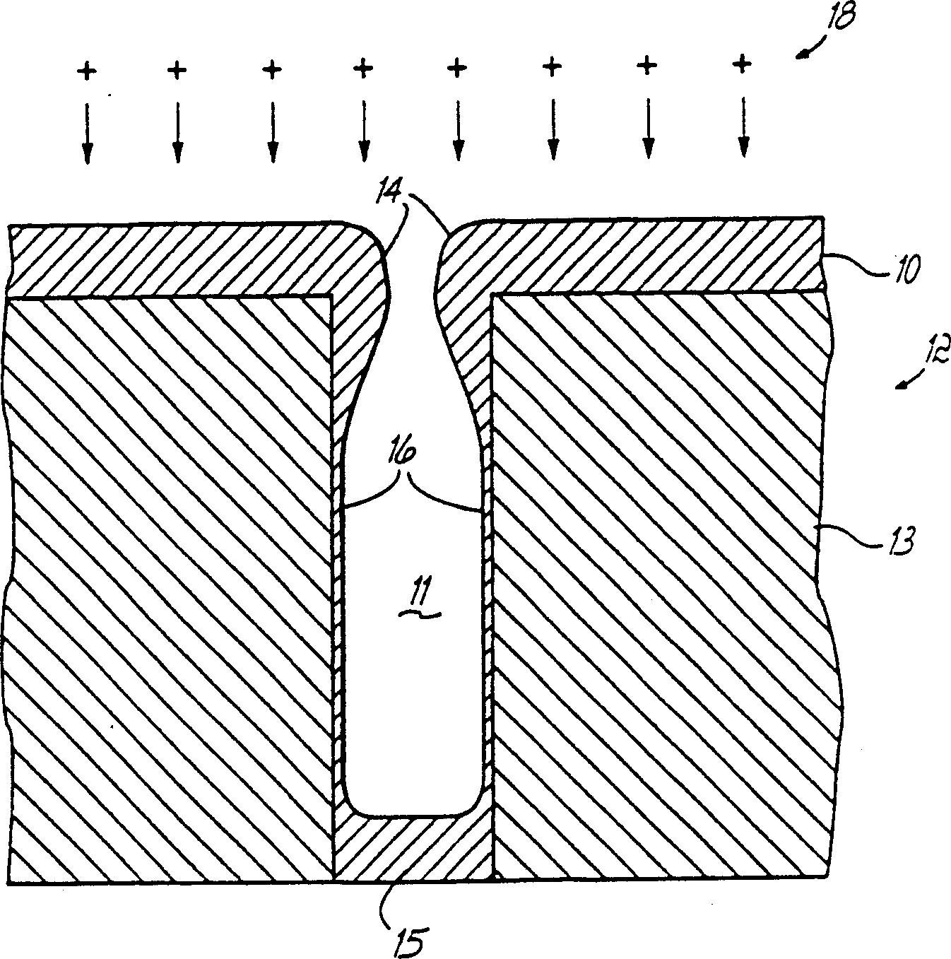
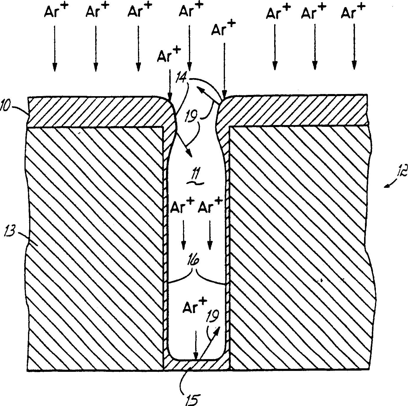
[0030] figure 1Denotes the deposition of a metal film 10 by iPVD in a channel structure 11 in a dielectric interlayer 13 of a semiconductor wafer 12 . As metal ions 18 are deposited on wafer 12, the metal deposit tends to thicken at the channel structure entrance, forming protruding structures 14. Likewise, the metal is deposited thicker at the bottom 15 of the trench structure 11 than at the sidewalls 16 . As the size of the channel structure decreases below 0.15 microns, but the thickness of the dielectric interlayer 13 does not decrease, the aspect ratio of the channel structure 11 will increase significantly, limiting the ability to reach the sidewall 16 of the channel structure 11. flow of metal ions14. For thinner depositions of less than 100 Å, the film deposited on the sidewalls 16 of the trench structure 11, especially for metal seed layers such as copper, tends to form agglomerated island structures. Gaps and discontinuities in the copper seed layer result in the ...


PUM


Abstract

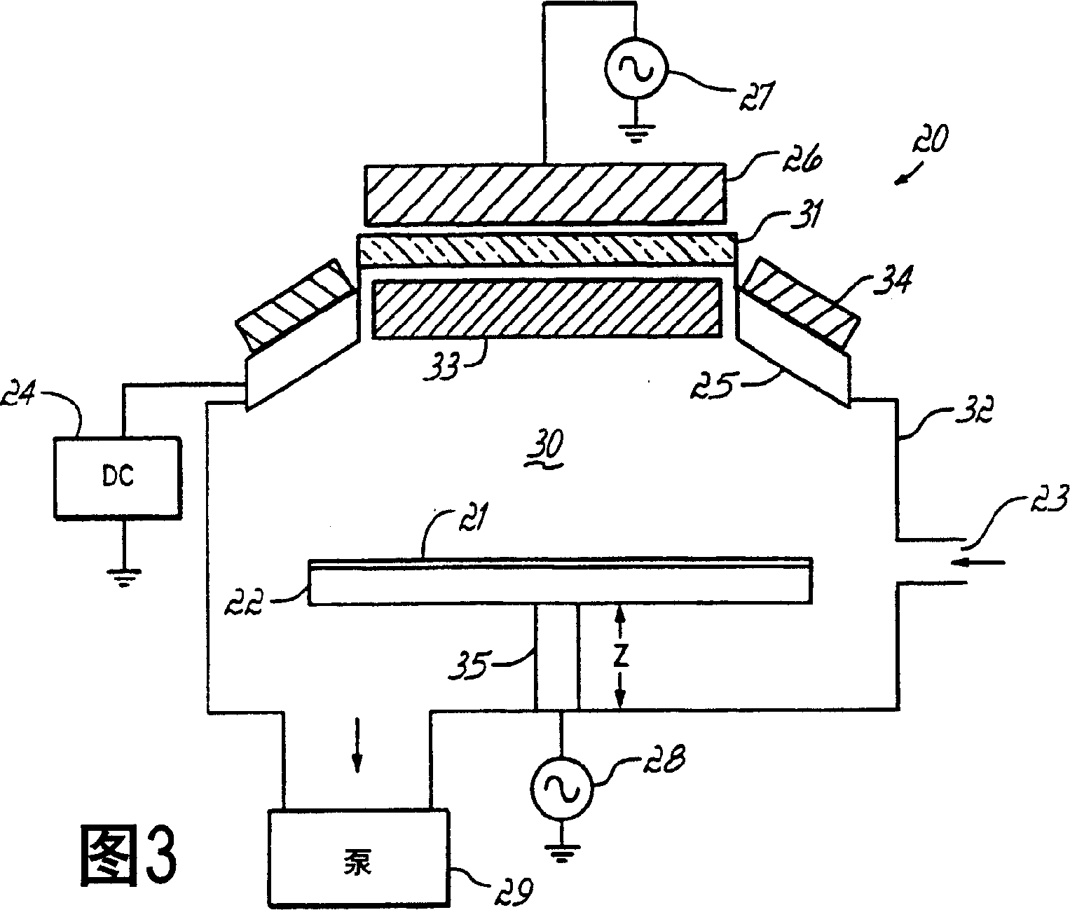
An iPVD apparatus (20) is programmed to deposit material (10) into high aspect ratio submicron features (11) on semiconductor substrates (21) by cycling between deposition and etch modes within a vacuum chamber (30). The modes operate at different power and pressure parameters. Pressure of more than 50 mTorr, for example, is used for sputtering material from a target while pressure of less than a few mTorr, for example, is used to etch. Bias power on the substrate is an order of magnitude higher for etching, producing several hundred volt bias for etching, but only a few tens of volts for deposition. The alternating etching modes remove deposited material that overhangs edges of features on the substrate, removes some of the deposited material from the bottoms (15) of the features, and resputters the removed deposited material onto sidewalls (16) of the features. The substrate (21) is cooled during deposition and etching, and particularly during etching to substantially below 0 DEG C. RF energy is coupled into the chamber (30) to form a high density plasma, with substantially higher RF power coupled during deposition than during etching. The substrate (21) is moved closer to the plasma source during etching than during deposition.

Description


Claims


Application Information

Patent Timeline
Owner TOKYO ELECTRON LTD
Learn More