
Driving circuit for semiconductor laser

A driving circuit and semiconductor technology, applied in the direction of semiconductor lasers, lasers, laser components, etc., can solve the problems of unusable and damaged semiconductor lasers

Inactive Publication Date: 2004-11-03
ALPS ALPINE CO LTD
View PDF1 Cites 8 Cited by
  • Summary
  • Abstract
  • Description
  • Claims
  • Application Information

AI Technical Summary

Problems solved by technology

As a result, there is a problem of damaging the semiconductor laser, so the conventional structure cannot be used in the so-called burst mode

Method used


Image

  • Driving circuit for semiconductor laser
  • Driving circuit for semiconductor laser
  • Driving circuit for semiconductor laser

Examples


Embodiment Construction

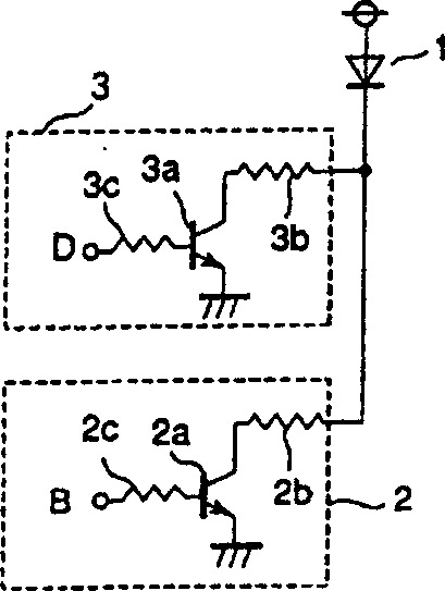
[0024] 32: According to Figure 1 to Figure 3 The driving circuit of the semiconductor laser of the present invention will be described. figure 1 Represent the structure of the drive circuit of the semiconductor laser of the present invention, figure 2 Indicates the light output characteristics of a semiconductor laser, image 3 Timing diagram showing modulation signal and bias current, Figure 5 Indicates other structures of the driving circuit of the semiconductor laser.

[0025] 33: in figure 1 , a specified voltage is applied to the anode of the semiconductor laser diode (single semiconductor laser) 1 . A bias current supply unit that supplies a bias current to the semiconductor laser 1 includes a first transistor (NPN type) 2 a connected in series with the semiconductor laser 1 . That is, the collector of the first transistor 2a is connected to the cathode of the semiconductor laser 1 through the resistor 2b for limiting the bias current, and the emitter is ground...


PUM


Abstract

Provided is a semiconductor laser drive circuit which is capable of preventing deterioration in an extinction ratio caused by a bias current so as to detect signals accurately and optimal for time-division telegraphy in a PON system or the like. The semiconductor laser drive circuit is equipped with a semiconductor laser, a bias current feed means which feeds a bias current to the semiconductor laser, and a modulating current feeding means which feeds a modulating current to the semiconductor laser on the basis of inputted modulating signals. The bias current is fed to the semiconductor laser at least during a period the modulating current is fed to the semiconductor laser, and stopped when the modulating current is stopped.

Description

[0001] 4: 5: Technical field [0002] 6: The present invention relates to a driving circuit for a semiconductor laser. 7: Background technology [0003] 8: The driving circuit of the conventional semiconductor laser is shown in Image 6 middle. A reference voltage Vref is applied to the base of a transistor 42 that flows a modulation current through the semiconductor laser 41, and its emitter is connected to the emitter of a transistor 43 to which a modulation pulse signal is input. The two emitters are connected to the collector of the transistor 44, and an operational amplifier 45 is arranged between the base and the emitter. The voltage of the emitter resistor 46 of the input transistor 44 on the operational amplifier 45 is negatively fed back to the inverting input terminal (-) by the thermistor 47, and the non-inverting input terminal (+) is grounded through the thermistor 48. [0004] 9: In the above structure, the continuous pulse signal turns on / off the transistors...

Claims


Application Information

Patent Timeline
IPC IPC(8): H01S5/068H01S5/042
CPCH01S5/0427H01S5/042E06B3/6205
Inventor 斋藤恭造
Owner ALPS ALPINE CO LTD
Learn More