Method for producing resin formed product, method for producing metal structure budy and resin forming product
A technology of resin molding and manufacturing method, which is applied to the manufacture of resin molded products, the manufacture of metal structures and the fields of resin molded products, can solve the problem of low production efficiency, high-priced silicon substrates, and inability to efficiently manufacture high-precision multi-segment structures Fuel cell separators, etc.
- Summary
- Abstract
- Description
- Claims
- Application Information
AI Technical Summary
Problems solved by technology
Method used
Image
Examples
Embodiment approach 1
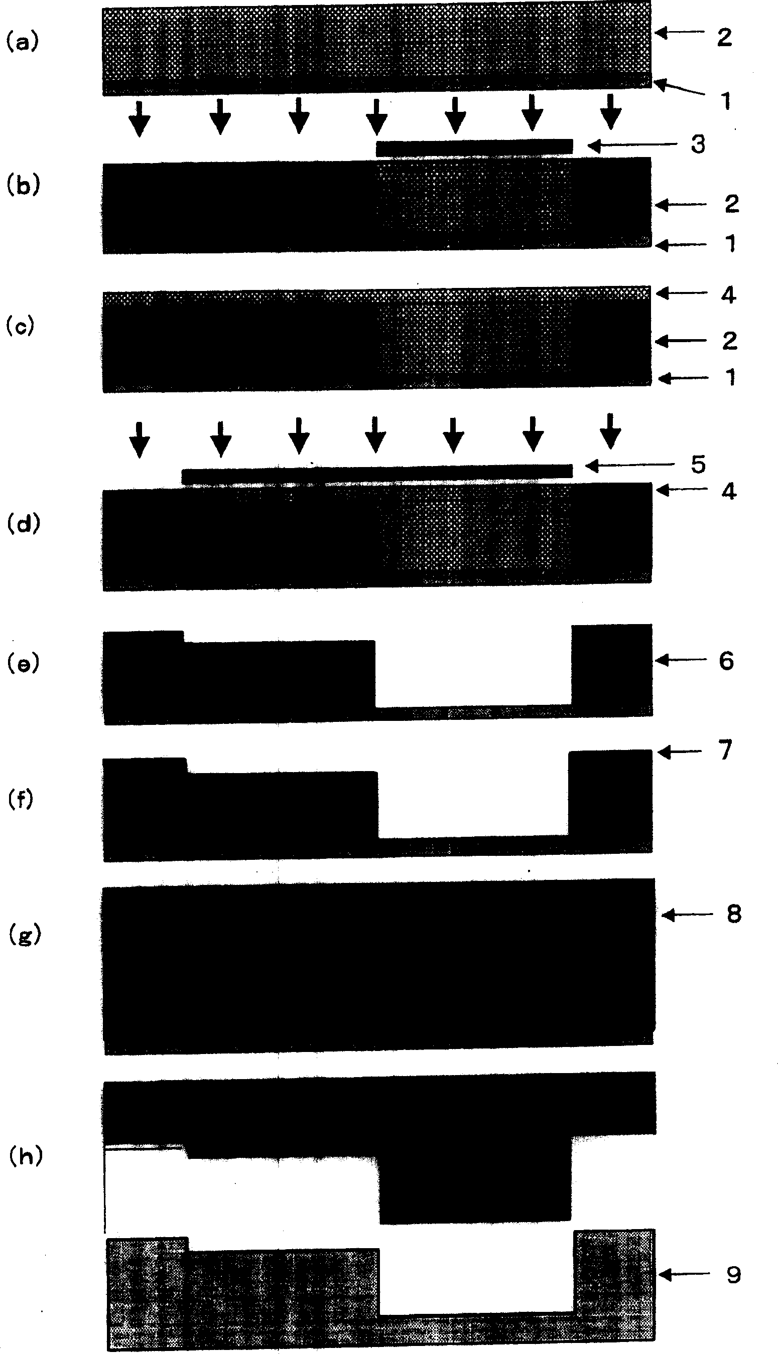
[0085] figure 1 The manufacturing process of the resin molded article in this embodiment is shown. The manufacturing apparatus used for realizing this embodiment is a well-known apparatus, and detailed description thereof will be omitted. refer to figure 1 The production method of this embodiment will be described. Furthermore, figure 1 An example using a chemically amplified negative resist is shown. In the resist pattern forming method of this scheme, the following processes are performed:
[0086] (i) forming the first resist layer on the substrate [ figure 1 (a)]
[0087] (ii) Alignment position of substrate and mask (A) [ figure 1 (b)]
[0088] (iii) Exposure of the first resist layer using mask (A) [ figure 1 (b)]
[0089] (iv) heat treatment of the first resist layer [ figure 1 (b)]
[0090] (v) forming a second resist layer on the first resist layer [ figure 1 (c)]
[0091] (vi) Alignment position of substrate and mask [ figure 1 (d)]
[0092] (vii) Exp...
Embodiment
[0154] According to the present invention, a method of forming a resin molded article will be described more specifically below with reference to the drawings. refer to figure 1 (a) First, the first resist coating based on an organic material ("PMER V-CA 3000PM" manufactured by Tokyo Ohka Industry Co., Ltd.) is performed on the substrate. And, refer to figure 1 (b) After forming the first resist layer, the substrate is aligned with the mask A processed into a desired mask pattern.
[0155] Then use a UV exposure device (Canon "PLA-501F" wavelength 365nm, exposure amount 300mJ / cm 2 ), and after exposing the first resist layer to UV light, heat treatment of the first resist layer was performed using a hot plate (100° C.×4 minutes).
[0156] refer to figure 1 (c) First, a second resist coating based on an organic material ("PMERN-CA 3000PM" manufactured by Tokyo Ohka Industry Co., Ltd.) is performed on the substrate. Then, refer to figure 1 (d) After forming the second resi...
Embodiment approach 2
[0173] use Figure 8 The method of manufacturing the metal structure (mold) and the resin molded article of the present embodiment will be described. Figure 8 It is a sectional view showing the manufacturing process of the metal structure (mold) of this embodiment. 51 is the substrate, 52 is the first layer resist, 53 is the first layer mask, 54 is the first intermediate structure, 55 is the second layer resist, 56 is the second layer mask, 57 is The second intermediate structure, 58 is a metal structure (mold). The mold is an example of the metal structure according to this embodiment. Since the same steps as those in the above-mentioned embodiment are the same as those described in Embodiment 1, description thereof will be omitted.
[0174] The resist coating step will be described. Firstly, a first-layer resist 52 based on an organic material (for example, “AZP 4400” manufactured by Kuraray, Japan) is coated on the substrate 51 . The resist 52 is a positive photosensi...
PUM
| Property | Measurement | Unit |
|---|---|---|
| diameter | aaaaa | aaaaa |
| thickness | aaaaa | aaaaa |
Abstract
Description
Claims
Application Information
 - R&D Engineer
- R&D Manager
- IP Professional
- Industry Leading Data Capabilities
- Powerful AI technology
- Patent DNA Extraction
Browse by: Latest US Patents, China's latest patents, Technical Efficacy Thesaurus, Application Domain, Technology Topic, Popular Technical Reports.
© 2024 PatSnap. All rights reserved.Legal|Privacy policy|Modern Slavery Act Transparency Statement|Sitemap|About US| Contact US: help@patsnap.com


