Microminiature power converter with multiple output
A power conversion device, ultra-small technology, applied in the direction of output power conversion device, DC power input conversion to DC power output, adjustment of electrical variables, etc., can solve the problems of small size, increased installation area, and increased installation cost
- Summary
- Abstract
- Description
- Claims
- Application Information
AI Technical Summary
Problems solved by technology
Method used
Image
Examples
Embodiment 1
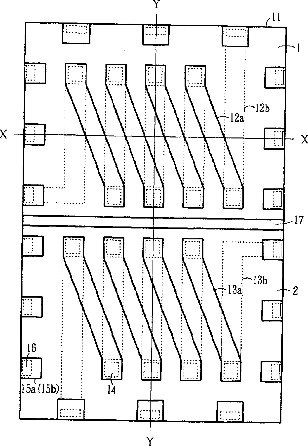
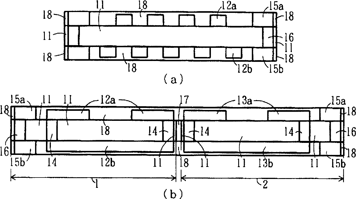
[0059] Fig. 1 and Fig. 2 are main part configuration diagrams of the multi-output ultra-small power conversion device according to Embodiment 1 of the present invention. Fig. 1 is a plan view of main parts when viewed from the upper part of an inductor composed of a thin-film magnetic induction element, and Fig. 2 (a) is a sectional view of main parts taken along line X-X in FIG. 1 , and FIG. 2( b ) is a sectional view of main parts taken along line Y-Y in FIG. 1 . In this example, the number of inductors is two. In these figures, not only the coil pattern of the inductor but also the connection terminals 15a, 15b constituted by the mounting terminals of the inductor for electrical connection are shown.
[0060] In FIG. 1 , coil conductors 12 a and 13 a are formed on a first main surface of a magnetic insulating substrate 11 , and coil conductors 12 b and 13 b are formed on a second main surface. The planar shape of the coil conductors 12b and 13b formed on the second main su...
Embodiment 2
[0084] FIG. 14 shows a method of manufacturing a multi-output ultra-small power conversion device according to Embodiment 2 of the present invention, and FIGS. 14( a ) to 14 ( c ) are cross-sectional views of main steps showing the sequence of steps. Here, a method of manufacturing a ferrite substrate is shown.
[0085] In Example 1, a resin was used as a material of the magnetic separation layer 17, but in this Example, a ceramic material was used. In the above-mentioned case of using the resin, the method is adopted to form the slit 41 in the ferrite substrate 11 in the process after the ferrite substrate 11 is sintered, and fill the slit 41 with the resin. In this embodiment, it is formed by simultaneously sintering ferrite and ceramics.
[0086] First, as shown in FIG. 14( a ), a printed circuit board 51 before ferrite sintering is formed.
[0087] Next, as shown in FIG. 14(b), a cutout 52 and through holes 53, 54 are formed in a printed circuit board 51 by a punching me...
Embodiment 3
[0094] Fig. 16 is a main part configuration diagram of a multi-output ultra-small power conversion device according to Embodiment 3 of the present invention. Fig. 16(a) is a plan view of main parts of the first inductor, and Fig. 16(b) is a main part plan view of the second inductor. Partial floor plan. These figures are plan views of main parts seen from the top of the inductor composed of a thin-film magnetic induction element.
[0095] Respectively, the plan view of the first inductor 60a in which the first coil conductors 62a, 62b and the first connection terminals 65a, 65b are formed on the first magnetic insulating substrate (hereinafter referred to as the first substrate 61a), and the first inductor 60a formed on the second magnetic insulating substrate A plan view of a second inductor 60b in which second coil conductors 63a, 63b and second connection terminals 66a, 66b are formed on a substrate (hereinafter referred to as a second substrate 61b). Also, 62a, 63a, 65a, ...
PUM
| Property | Measurement | Unit |
|---|---|---|
| Thickness | aaaaa | aaaaa |
| Thickness | aaaaa | aaaaa |
Abstract
Description
Claims
Application Information
 - R&D Engineer
- R&D Manager
- IP Professional
- Industry Leading Data Capabilities
- Powerful AI technology
- Patent DNA Extraction
Browse by: Latest US Patents, China's latest patents, Technical Efficacy Thesaurus, Application Domain, Technology Topic, Popular Technical Reports.
© 2024 PatSnap. All rights reserved.Legal|Privacy policy|Modern Slavery Act Transparency Statement|Sitemap|About US| Contact US: help@patsnap.com


