
Display appts.

A display device, an input display technology, applied to lighting devices, static indicators, cathode ray tube indicators, etc., can solve the problem of pixel aperture ratio reduction, achieve an increase in aperture ratio, simplify control circuits and control wiring, reduce The effect of manufacturing costs

Active Publication Date: 2004-05-26
SAMSUNG DISPLAY CO LTD
View PDF2 Cites 3 Cited by
  • Summary
  • Abstract
  • Description
  • Claims
  • Application Information

AI Technical Summary

Problems solved by technology

[0003] However, in the driving method described in "An Innovative Pixel-Driving Scheme for 64-Level Gray-Scale Full-Color Active Matrix OLED Displays", the switching switch and the wiring for triangular wave supply are designed in the pixel, resulting in pixel Reduced aperture ratio
The method described in U.S. Patent No. 6,229,508 also reduces the aperture ratio of the pixel due to the switch and the wiring for supplying the precharge voltage in the pixel.

Method used


Image

  • Display appts.
  • Display appts.
  • Display appts.

Examples


no. 1 example

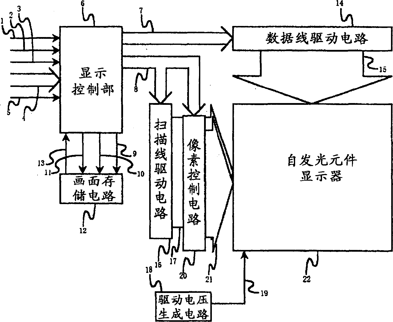
[0022] figure 1 It is a block diagram illustrating the system configuration of the display device according to the first embodiment of the present invention. figure 1 Among them, 1 is a vertical synchronous signal, 2 is a horizontal synchronous signal, 3 is a data enabling signal, 4 is a display data (can be an animation or a still picture), and 5 is a synchronous clock. Vertical synchronous signal 1 is a signal representing a display period (1 frame period), horizontal synchronous signal 2 is a signal of a horizontal period, and data enable signal 3 is a signal representing a valid period of display data 4 (display valid period), All signals are input synchronously with the synchronous clock 5 .

[0023] In this embodiment, a case where one screen size of these display data is sequentially transmitted from the upper left in a raster scan format, and the information of one pixel size is composed of 6-bit gray scale data will be described below. 6 is a display control unit, 7...

no. 2 example

[0053] Refer below Figure 9 and Figure 10 A second embodiment of the present invention will be described in detail. Figure 9 It is a block diagram illustrating a system configuration of a display device according to a second embodiment of the present invention. Figure 9 Among them, 1 is a vertical synchronous signal, 2 is a horizontal synchronous signal, 3 is a data enable signal, 4 is a display data, and 5 is a synchronous clock, all of which are the same as those in the first embodiment. 83 is a built-in display control unit for flyback period control, 84 is a built-in data line control signal for flyback period control, 8 is a scan line control signal, 9 is a storage / read command signal, 10 is a storage / read address, and 11 is a storage Data, 12 is the screen storage circuit, 13 is the screen readout data. The built-in display control unit 83 controls the retrace period, similarly to the first embodiment, while generating the scanning line control signal 8, the stora...


PUM


Abstract

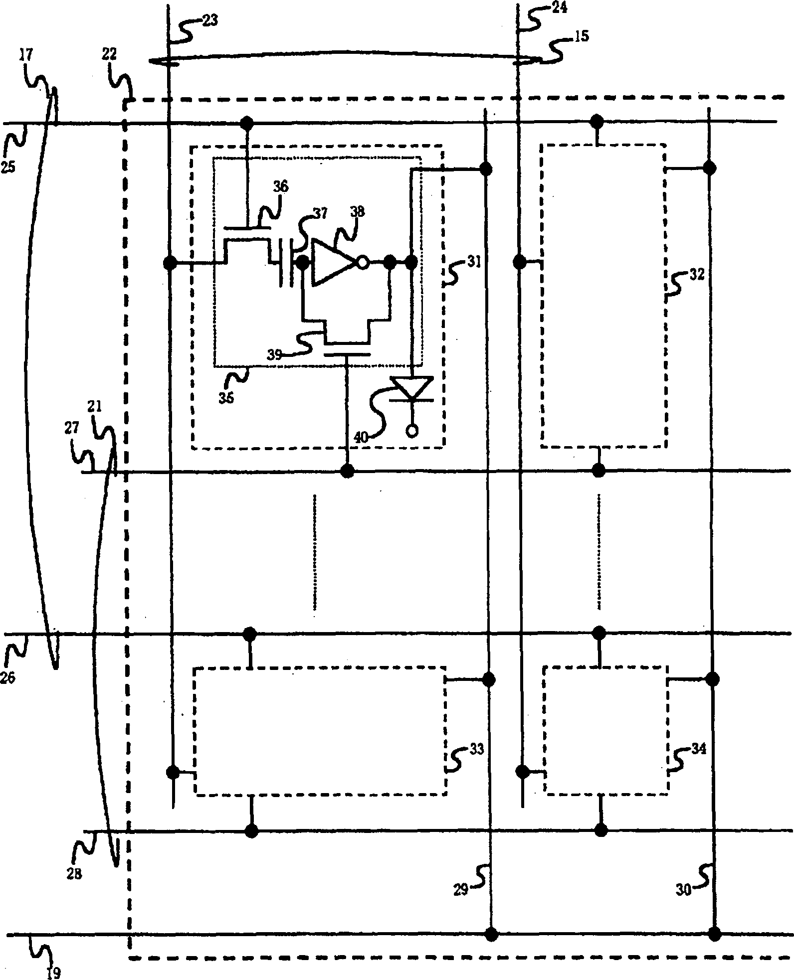
A display apparatus comprises a self-luminous device display having a plurality of light emitting elements arranged in a matrix, a drive voltage generation circuit to generate a drive voltage signal for driving light emitting elements, a blanking period control-included data line drive circuit which controls the drive voltage either according to or irrelevantly to the display data, a scan line drive circuit to determine which light emitting elements to drive, and a pixel control circuit to control voltage write to pixels.

Description

technical field [0001] The present invention relates to a display device capable of controlling the amount of current applied to a display element, or controlling the brightness corresponding to the light emission time, and particularly relates to self-luminescence represented by light-emitting diodes (LEDs), organic EL (electroluminescence), and the like. The element is a display device constituted as a display element. Background technique [0002] Various display methods have been proposed as flat panel display devices typified by cathode ray tubes. In particular, organic EL display devices, field emission display devices (FED), plasma display devices, and the like have attracted attention as so-called self-luminous display devices in which display elements emit light by themselves. Regarding the driving of an organic EL display device as one of the self-luminous display devices, a method written in "An Innovative Pixel-Driving Scheme for 64-Level Gray-Scale Full-Color A...

Claims


Application Information

Patent Timeline
Patent Type & Authority Applications(China)
IPC IPC(8): H01L51/50G09G3/20G09G3/30G09G3/32G09G5/00H05B33/14
CPCG09G2300/0465G09G2310/0259G09G3/2014G09G3/3208G09G3/20G09G2310/0275G09G3/30
Inventor 笠井成彦粟仓博基佐藤敏浩秋元肇
Owner SAMSUNG DISPLAY CO LTD
Learn More