Display panel
A technology of display panel and display area, applied in static indicators, identification devices, instruments, etc., can solve the problems of line insulation breakdown, characteristic deterioration, etc.
- Summary
- Abstract
- Description
- Claims
- Application Information
AI Technical Summary
Problems solved by technology
Method used
Image
Examples
Embodiment Construction
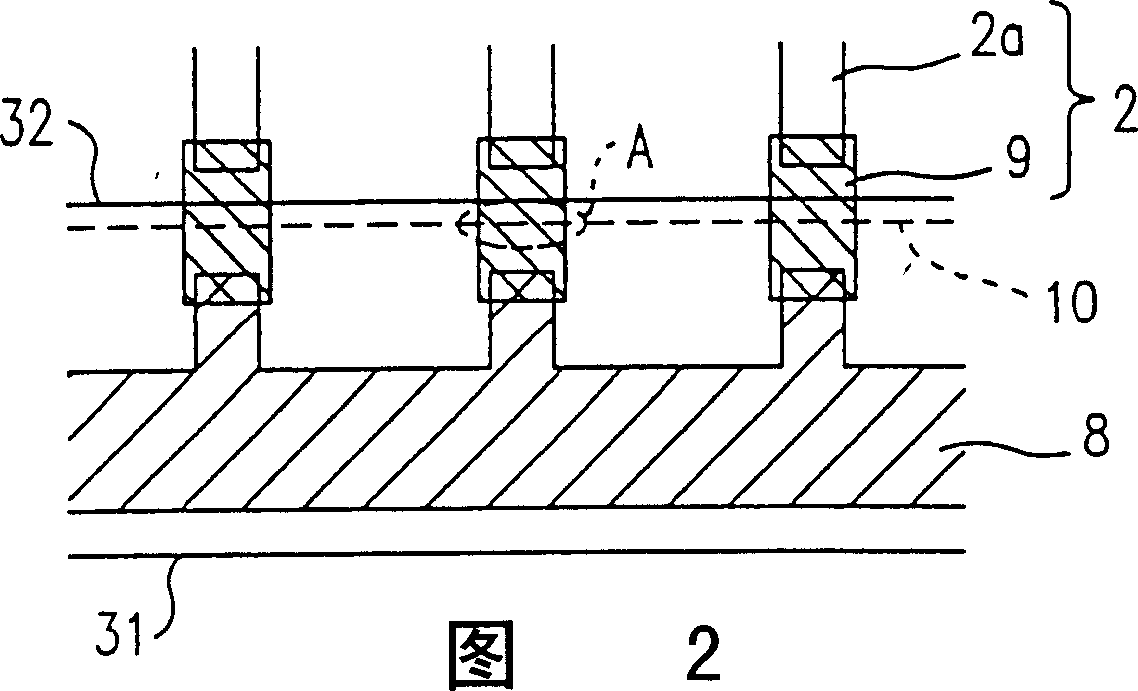
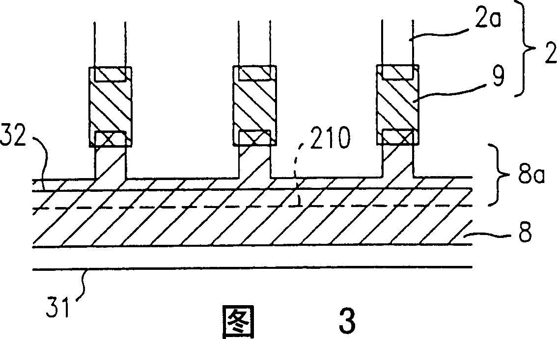
[0043] Thereafter, the present invention will be described by way of embodiments with reference to the accompanying drawings. In the drawings for describing examples of the present invention, elements whose functions are the same as those in conventional examples are denoted by the same reference numerals.
[0044] (Example 1)
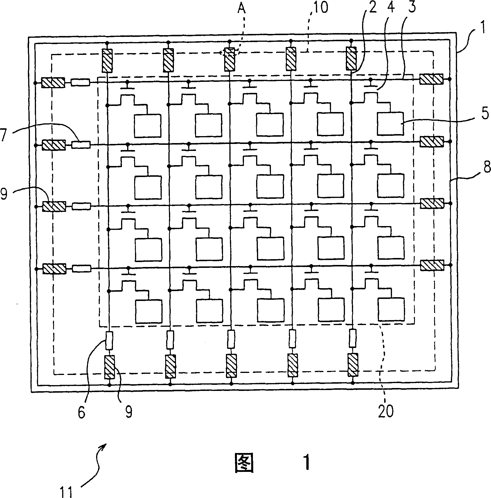
[0045] FIG. 1 shows an equivalent circuit of an active matrix substrate 11 in a display panel according to Example 1 of the present invention.
[0046] The active matrix substrate 11 includes a transmissive substrate 1 made of a glass plate or the like, and a plurality of signal lines 2 and a plurality of scanning lines 3 crossing each other through insulating films (not shown). Active matrix substrate 11 also includes TFT 4 and pixel electrodes 5 as switching elements in the vicinity of intersections between signal lines 2 and scanning lines 3 . A display area is defined by a plurality of pixel electrodes 5 arranged in a matrix layout. Each pixel e...
PUM
 Abstract
Description
Claims
Application Information
 - R&D
- Intellectual Property
- Life Sciences
- Materials
- Tech Scout
- Unparalleled Data Quality
- Higher Quality Content
- 60% Fewer Hallucinations
Browse by: Latest US Patents, China's latest patents, Technical Efficacy Thesaurus, Application Domain, Technology Topic, Popular Technical Reports.
© 2025 PatSnap. All rights reserved.Legal|Privacy policy|Modern Slavery Act Transparency Statement|Sitemap|About US| Contact US: help@patsnap.com


