A method for individualised marking of circuit boards

A technology for distinguishing marks and circuit boards, applied in circuit inspection/identification, removal of conductive materials by chemical/electrolytic methods, circuits, etc., can solve problems such as unsuitable exposure technology

Inactive Publication Date: 2003-08-20
芳诺・萨尔米
View PDF4 Cites 2 Cited by
  • Summary
  • Abstract
  • Description
  • Claims
  • Application Information

AI Technical Summary

Problems solved by technology

The exposure techniques described in this bulletin are not suitable for distinguishing marks, i.e. markings that differ from one product to another by photolithography

Method used


Image

  • A method for individualised marking of circuit boards
  • A method for individualised marking of circuit boards
  • A method for individualised marking of circuit boards

Examples


Embodiment Construction

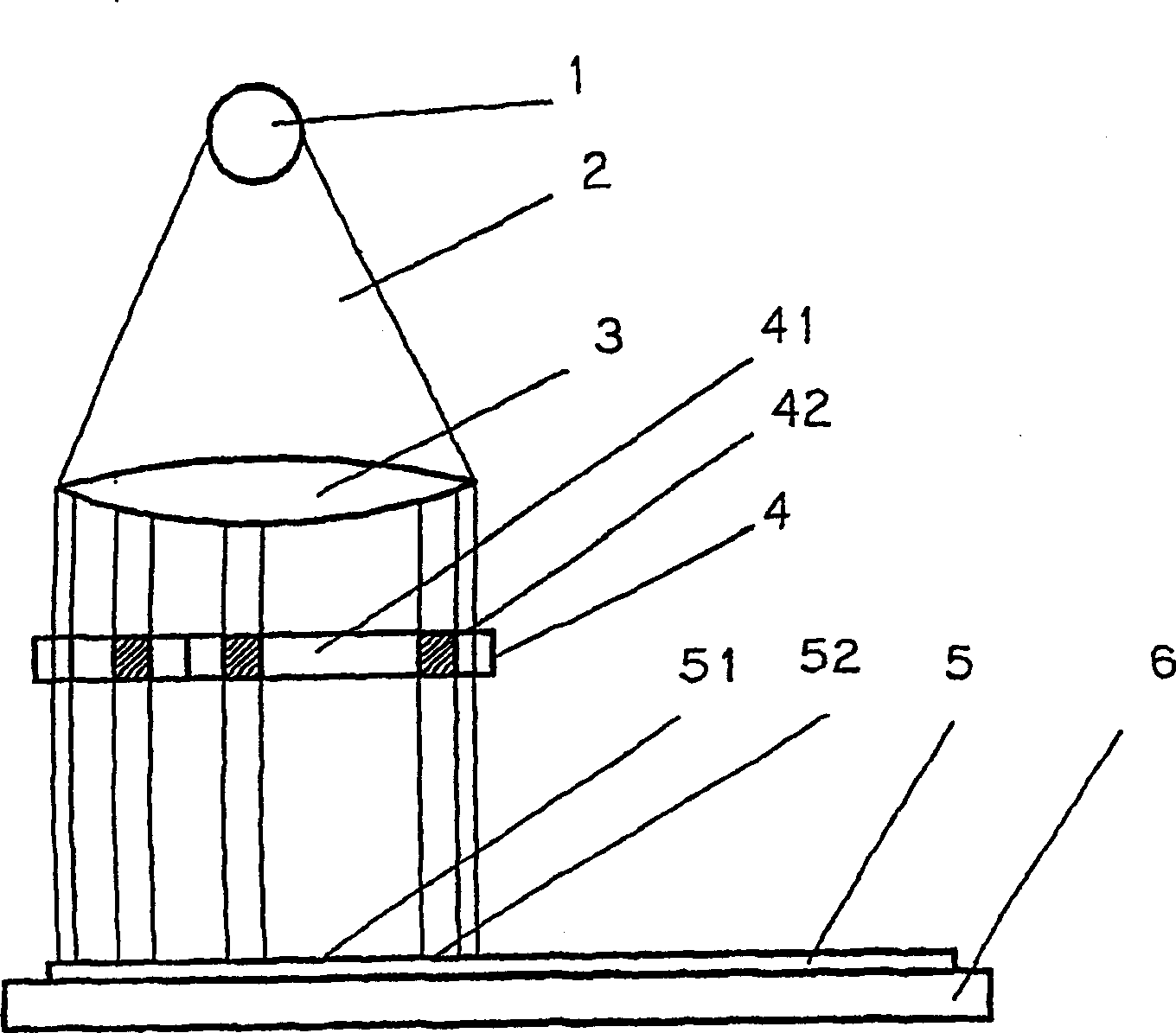
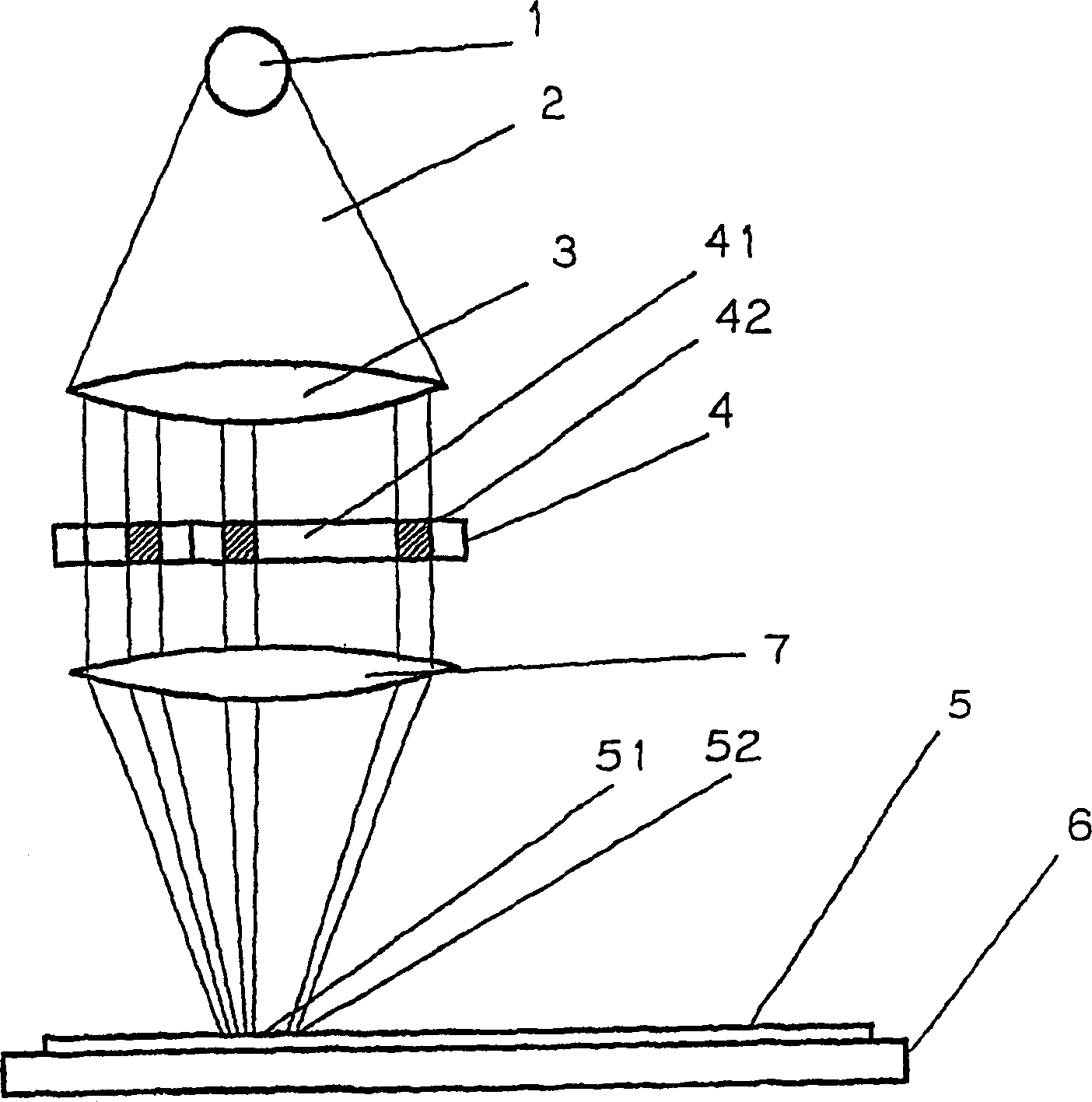
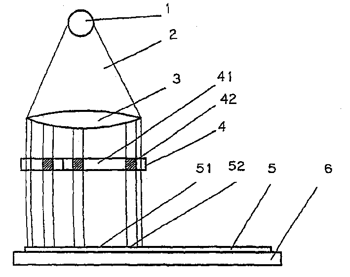
[0037] In the figures, the same reference numerals denote mutually corresponding elements. exist figure 1 In, reference numeral 1 denotes a light source, and reference numeral 2 denotes its light beam, which is directed to a photosensitive surface portion 5 of a circuit board 6 to be marked. An optical device 3 and a device 4 with adjustable transparency are arranged in the light beam 2 of the light source 1 . The device 4 comprises a region 41 which is in the direction of propagation of the light and which allows the passage of light, and a region 42 which does not allow the passage of light or whose transparency is substantially lower than that of the region 41 .

[0038] The shape and position of the areas 41 and 42 are selected so that by means of them a pattern corresponding to the desired marking can be formed on the photosensitive surface 5 of the circuit board 6 . The figures do not show the means for adjusting the shape and / or position of the regions 41 and 42 . In...


PUM


Abstract

A method for individualised marking of electronic components in electronics manufacture, such as circuit boards. On the photosensitive surface required for manufacturing the blanks is exposed, on each blank, a machine-readable pattern, which is subsequently used in the manufacture of the product itself, for individualising the blanks in question.

Description

technical field [0001] The invention relates to a method for distinctively marking printed circuit boards by exposure methods in the manufacture of circuit boards. Background technique [0002] In industrial manufacturing processes, especially in the assembly industry, it is important that the components used in the assembly can be identified individually for each respective component. Instructions for assembly and / or for carrying out tests and the inspections associated therewith are also required during assembly. There is also often a need to be able to track the lot size of a component or the date a component was manufactured. To solve these identification problems, the components are marked, for example by gluing labels on them, marking them manually, by means of a laser or inkjet printer, or by means of other corresponding marking methods. In certain assembly processes, the assembly line includes at the beginning a marking unit in which the component or certain compon...

Claims


Application Information

Patent Timeline
IPC IPC(8): G03F7/20G03C11/02H01L21/00H05K1/02H05K3/00H05K3/06
CPCH05K2203/0551H05K2201/09927H05K1/0266H05K3/064H05K2201/09781G03C11/02H05K3/0082H01L21/67282H05K3/00
Inventor 芳诺·萨尔米
Owner 芳诺・萨尔米
Why Eureka
Try Eureka