Display device and electron instrument
A technology for display devices and electronic instruments, which is applied to lighting devices, electric solid state devices, circuits, etc., can solve the problems of decreased contrast and color stains of display devices, and achieves the effect of improving contrast and improving visual recognition.
- Summary
- Abstract
- Description
- Claims
- Application Information
AI Technical Summary
Problems solved by technology
Method used
Image
Examples
Embodiment 1
[0078] Next, Embodiment 1 of the present invention will be described with reference to the drawings.
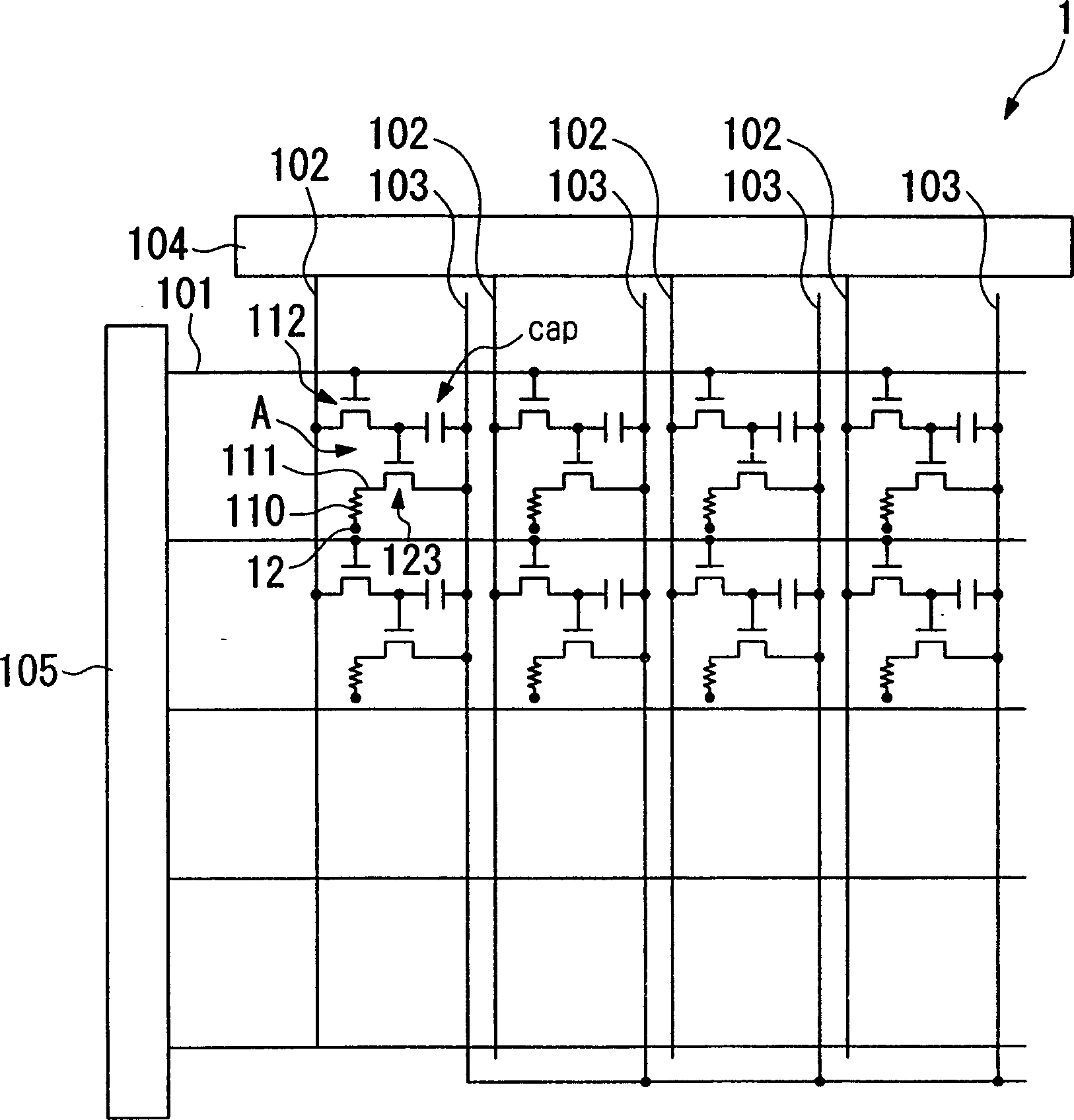
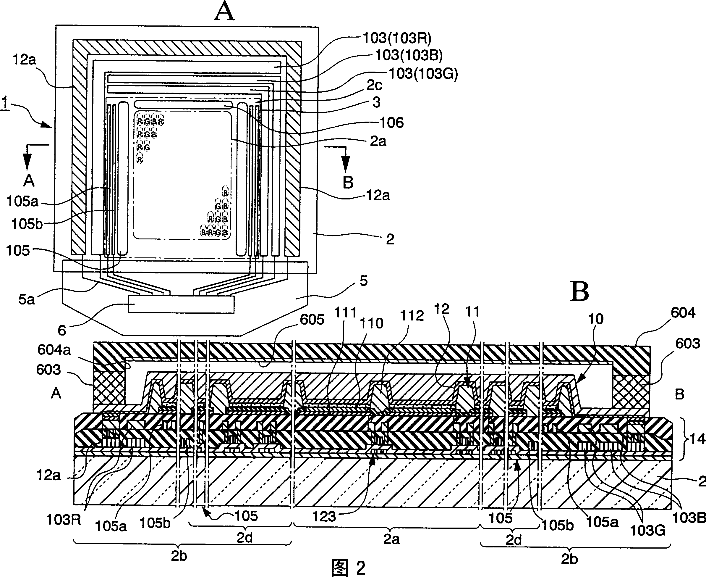
[0079] figure 1 A schematic plan view showing the wiring structure of the display device of this embodiment, and FIG. 2 shows a schematic plan view and a schematic cross-sectional view of the display device of this embodiment.
[0080] like figure 1 As shown, the display device 1 of this embodiment has a structure in which a plurality of scanning lines 101, a plurality of signal lines 102 extending in a direction intersecting the scanning lines 101, and a plurality of power supply lines 103 extending in parallel with the signal lines 102 are respectively provided. , and pixel regions A are provided near the intersections of the scanning lines 101 and the signal lines 102 .
[0081] On the signal line 102, a data-side driver circuit 104 having a shift register, a level shifter, a video line, and an analog switch is connected. In addition, a scanning line-side driver circu...
Embodiment 2
[0277] Next, Embodiment 2 of the present invention will be described with reference to the drawings.
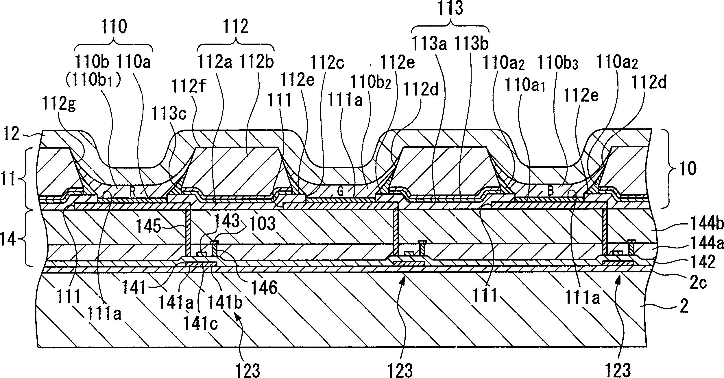
[0278] Figure 21 It is a cross-sectional view showing the main part of the display device of the second embodiment.
[0279] like Figure 21 As shown, the structure of the display device of this embodiment is that the circuit element portion 14 formed with circuits such as TFTs, the light emitting element portion 211 formed with a light emitting layer, and the cathode 12 are sequentially stacked on the substrate 2 .
[0280] In the display device of this embodiment, as in Embodiment 1, the light emitted from the functional layer 110 to the substrate 2 side passes through the circuit element portion 14 and the substrate 2, and is emitted to the lower side of the substrate 2 (observation the other side), and the light emitted from the functional layer 110 to the opposite side of the substrate 2 is reflected by the cathode 12, passes through the circuit element part 14 and th...
Embodiment 3
[0294] Next, Embodiment 3 of the present invention will be described with reference to the drawings.
[0295] Figure 22 It is a sectional view showing the main part of the display device of the third embodiment.
[0296] like Figure 22 As shown, the structure of the display device of this embodiment is that the circuit element portion 14 formed with circuits such as TFTs, the light emitting element portion 311 formed with a light emitting layer, and the cathode 12 are sequentially stacked on the substrate 2 .
[0297] In the display device of this embodiment, as in the first and second embodiments, the light emitted from the functional layer 110 to the substrate 2 side passes through the circuit element portion 14 and the substrate 2, and is emitted to the lower side of the substrate 2. (observer side), and the light emitted from the functional layer 110 to the opposite side of the substrate 2 is reflected by the cathode 12, passes through the circuit element part 14 and t...
PUM
 Abstract
Description
Claims
Application Information
 - R&D
- Intellectual Property
- Life Sciences
- Materials
- Tech Scout
- Unparalleled Data Quality
- Higher Quality Content
- 60% Fewer Hallucinations
Browse by: Latest US Patents, China's latest patents, Technical Efficacy Thesaurus, Application Domain, Technology Topic, Popular Technical Reports.
© 2025 PatSnap. All rights reserved.Legal|Privacy policy|Modern Slavery Act Transparency Statement|Sitemap|About US| Contact US: help@patsnap.com


