Eureka AIR delivers breakthrough ideas for toughest innovation challenges, trusted by R&D personnel around the world.

Contactor device

A contactor and terminal connection technology, applied in the direction of coupling devices, measuring devices, contact parts, etc., can solve problems such as difficulty in manufacturing contactors, contactor manufacturing errors, machine stop position errors, etc.

Inactive Publication Date: 2002-11-13
木本军生
View PDF0 Cites 2 Cited by
  • Summary
  • Abstract
  • Description
  • Claims
  • Application Information

AI Technical Summary

Problems solved by technology

As a result, the occupied space allocated to the deformation portion of one contact becomes insufficient, making it difficult to manufacture a contact with an appropriate spring constant
If the elastic deformation of the contactor is small, the action range is narrow, and when there is a manufacturing error of the contactor, or when the contactor produces a machine stop position error during the contact action, the gap between the contactor and the electrode pad cannot be obtained. Appropriate contact voltage, this is also a problem to be solved

Method used


Image

  • Contactor device
  • Contactor device
  • Contactor device

Examples


Embodiment 1

[0053] The first embodiment of the present invention is shown in Fig. 4 to Fig. 21 . FIG. 4 is an arrangement diagram of electrode pads on a wafer base, and FIG. 5 is an arrangement diagram of electrode pads of a circuit network. As shown in FIG. 4 , on the wafer substrate 19 , the electrode pads 191 are arranged in a row and arranged in a rectangular (square) shape as a whole, and some parts of the four corners are not provided with electrode pads. As shown in FIG. 5 , in the circuit network 20 , the electrode pads 120 are arranged in a row and arranged in a rectangular shape as a whole. The electrode pads 191 of a chip of the above-mentioned wafer substrate 19 and the electrode pads 120 of the circuit network 20 are formed to face each other, and have a consistent positional relationship. Embodiment 1 is an illustration for a contactor having the following characteristics: the contactor is effective in the electrical connection and electrical conduction between the aforemen...

Embodiment 2

[0063] 22 to 27 are diagrams showing a second embodiment of the present invention. In Embodiment 2, the case where the electrode pads are arranged in a staggered manner is taken as an example for description.

[0064] As shown in FIG. 22 , the first and second vertical contactors 112 , 212 are in a pair structure such that the outer contactor 22 and the inner contactor 21 are arranged opposite to the electrode pad 191 . In other words, the beam portion from the input portion 13, the output portion 14 of the vertical contactor 112, 212 to the deformation portion 15 extends to the outer electrode pads 191 arranged in a quadrangular shape; and the above-mentioned vertical contactor 112, 212 is They are arranged opposite to the outer electrode pads 191 arranged in a zigzag pattern. Furthermore, the beam portions from the input portion 13, the output portion 14, and the deformation portion 15 of the vertical contactors 112 and 212 extend to the inner electrode pads 191 arranged in...


PUM


Abstract

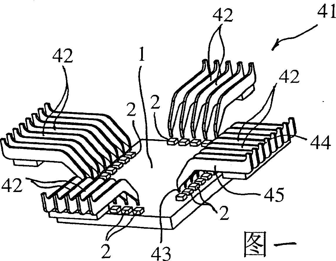
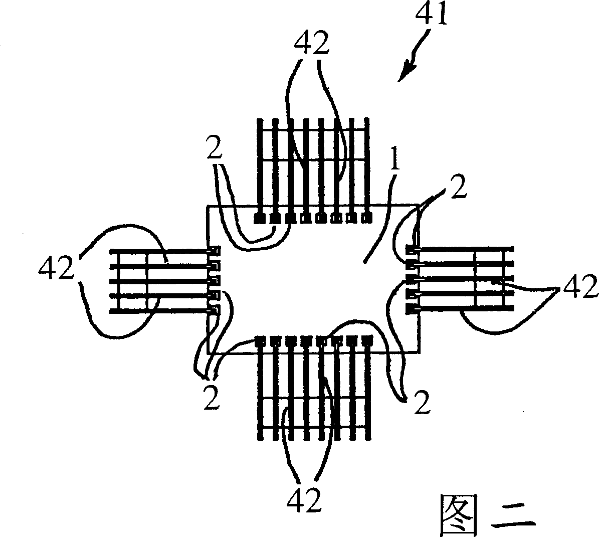
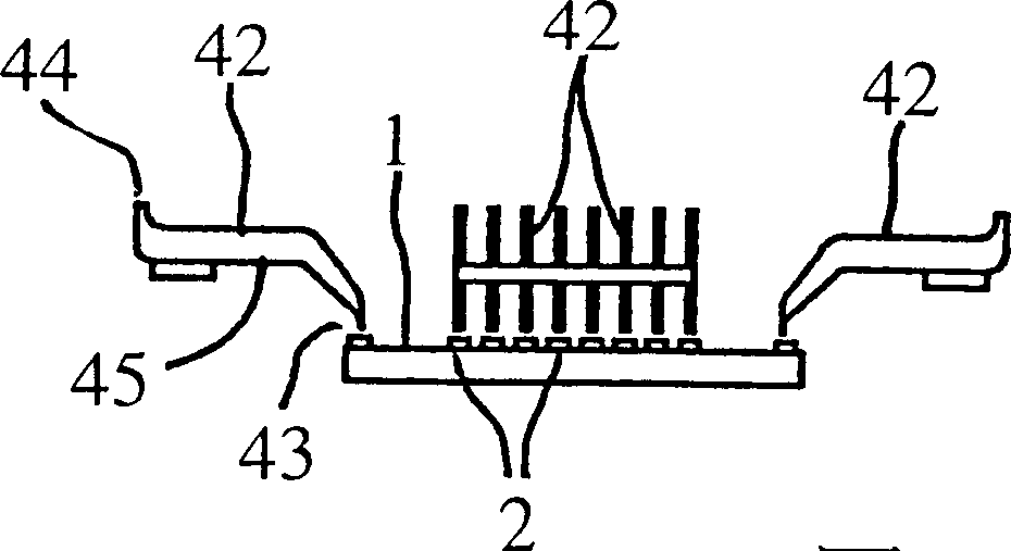
The invention discloses a contactor device for detecting the electronic characteristics of electronic components such as semiconductor integrated circuit chips. The space on the chip under test is occupied by the contactor corresponding to the chip under test, and the contactor will not invade the space on other chips under test. Therefore, the present invention includes: a horizontal parallel contactor group including a plurality of first vertical contactors; and a vertical parallel contactor group including a plurality of second vertical contactors. The horizontal parallel contactor group and the vertical parallel contactor group occupy different deformation spaces on the plane area of ​​the tested chip, and are converged in the plane area of ​​the tested chip.

Description

technical field [0001] The invention relates to a contactor device, especially a contactor device for detecting the electronic characteristics of original devices such as semiconductor integrated circuit chips or liquid crystal components, especially related to the contactor device for detecting IC chips on a wafer base . Background technique [0002] The traditional method of detecting a semiconductor integrated circuit chip (IC chip) or LSI chip (also an integrated circuit chip) is: contact the contactor with the terminal of the chip under test such as an IC chip or LSI chip and conduct electricity to implement electronic characteristics. detection. Commonly used contactors are single arm contactors or vertical action contactors. If a single-arm contactor is used, the contactor is arranged in the lateral direction of the substrate, and the output part of the contactor is connected to the pattern wiring formed on the substrate. If a vertical operation type contactor is u...

Claims


Application Information

Patent Timeline
Patent Type & Authority Applications(China)
IPC IPC(8): G01R31/26G01R1/06G01R1/067G01R1/073H01L21/66
CPCG01R1/07314G01R1/07357G01R1/06727G01R1/06738G01R1/073
Inventor 木本军生高井新吉
Owner 木本军生
Why Eureka
Eureka Blog
Learn More