Wafer carrier structure for chemical and mechanical grinder
A technology of grinding device and chemical machinery, applied in grinding device, abrasive surface adjusting device, positioning device, etc., can solve the problems of occupying space of chemical mechanical grinding machine, difficult maintenance, complicated structure of grinding pad adjuster, etc., and achieve cost saving The effect of manpower, simplification of consumables, and effective utilization
- Summary
- Abstract
- Description
- Claims
- Application Information
AI Technical Summary
Problems solved by technology
Method used
Image
Examples
no. 1 example
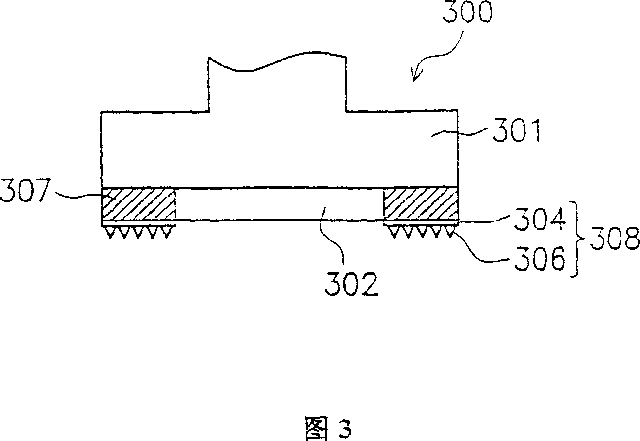
[0042] As shown in FIG. 3 and FIG. 4 , they are schematic diagrams illustrating the structure of the wafer carrier of the chemical mechanical polishing device according to the first embodiment of the present invention.
[0043] Please refer to Fig. 3, the structure of the wafer carrier 300 of the present embodiment includes: a grinding head 301 and a grinding pad regulator 308, wherein a wafer 302 is fixed on a wafer edge pressing ring 307 at the bottom of the grinding head 301 inside, while the polishing pad adjuster 308 is fixed on the surface of the wafer edge pressing ring 307 . Wherein the structure of the wafer carrier 300 also includes a wafer carrier attached with an elastic porous carrier film (not shown), so as to press the wafer 302 into the wetted carrier film to fix the wafer 302 . Another wafer carrier 300 structure also includes a vacuum hole (not shown), using a vacuum negative pressure to hold the wafer 302, and injecting nitrogen positive pressure during gri...
no. 2 example
[0048] As shown in FIG. 5 and FIG. 6 , they are schematic diagrams showing the structure of the wafer carrier of the chemical mechanical polishing device according to the second embodiment of the present invention.
[0049]Please refer to Fig. 5, the structure of the wafer carrier 400 of the present embodiment includes: a grinding head 401 and a grinding pad regulator 408, wherein a wafer 402 is fixed on a wafer edge pressing ring 407 at the bottom of the grinding head 401 Inside, the polishing pad regulator 408 is connected to the side of the polishing head 401 , and a brush surface 405 of the polishing pad regulator 408 is parallel to the surface of the wafer edge pressing ring 407 . Wherein the structure of the wafer carrier 400 also includes a wafer carrier attached with an elastic porous carrier film (not shown), so as to press the wafer 402 into the wetted carrier film to fix the wafer 402 . Another structure of the wafer carrier 400 also includes a vacuum hole (not sho...
no. 3 example
[0054] As shown in FIG. 7 and FIG. 8 , they are schematic diagrams illustrating the structure of a wafer carrier of a chemical mechanical polishing device according to a preferred embodiment of the present invention.
[0055] Referring to FIG. 7 , the structure of the wafer carrier 500 of this embodiment includes: a polishing head 501 and a polishing pad adjuster 508 . One of the wafers 502 is fixed inside a wafer edge pressing ring 507 at the bottom of the grinding head 501 , and the polishing pad adjuster 508 is embedded on the surface of the wafer edge pressing ring 507 . Wherein the structure of the wafer carrier 500 also includes a wafer carrier attached with an elastic porous carrier film (not shown), so as to press the wafer 502 into the wet carrier film to fix the wafer 502 . Another structure of the wafer carrier 500 also includes a vacuum hole (not shown), using a vacuum negative pressure to hold the wafer 502, and injecting a nitrogen positive pressure during grind...
PUM
 Abstract
Description
Claims
Application Information
 - R&D Engineer
- R&D Manager
- IP Professional
- Industry Leading Data Capabilities
- Powerful AI technology
- Patent DNA Extraction
Browse by: Latest US Patents, China's latest patents, Technical Efficacy Thesaurus, Application Domain, Technology Topic, Popular Technical Reports.
© 2024 PatSnap. All rights reserved.Legal|Privacy policy|Modern Slavery Act Transparency Statement|Sitemap|About US| Contact US: help@patsnap.com


