Method of forming sub-micron-size structures over a substrate

A sub-micron and substrate technology, applied in the direction of microstructure technology, microstructure devices, manufacturing microstructure devices, etc., can solve the problems of lack of nucleation position arrangement and arrangement ability

Inactive Publication Date: 2007-05-02
INTEL CORP
View PDF4 Cites 0 Cited by
  • Summary
  • Abstract
  • Description
  • Claims
  • Application Information

AI Technical Summary

Problems solved by technology

Although structures can be generated, there are issues related to the selective growth of these nanowires or nanotubes at specific locations on the substrate due to the lack of ability to align and place nucleation sites

Method used


Image

  • Method of forming sub-micron-size structures over a substrate
  • Method of forming sub-micron-size structures over a substrate
  • Method of forming sub-micron-size structures over a substrate

Examples


Embodiment Construction

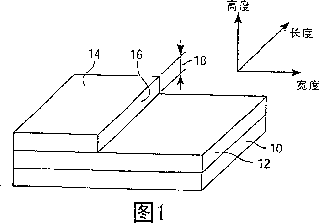
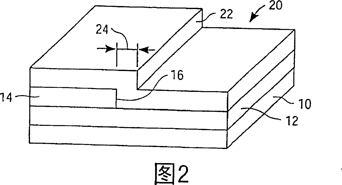
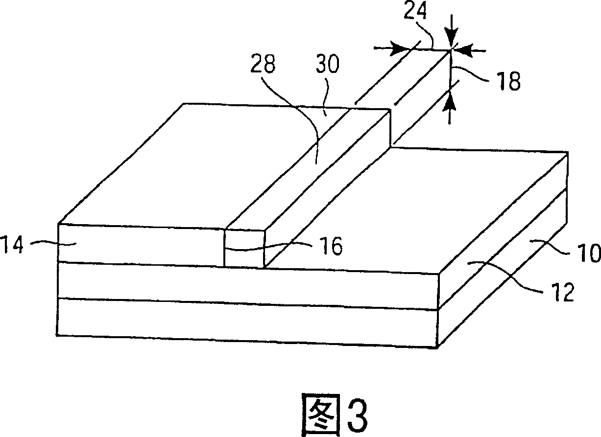
[0023] A method for forming submicron sized structures on a substrate is provided. A width-defining step is formed on the substrate. A width-defining layer is formed on an edge of the width-defining step. The width-defining layer is etched back to leave a spacer adjacent to the width-defining step. A length-defining step is formed on the substrate. A length-defining layer is formed on the edge of the length-defining step. The length-defining layer is etched back to leave a spacer proximate to the first edge of the length-defining step and spanning a first portion of the spacer left by the width-defining layer. Then remove the length-defining step. The spacers left by the width-defining layer are then etched using the spacers left by the length-defining layer as a mask to form the structure.

[0024] Figure 1 illustrates an initial process for forming a structure according to an embodiment of the invention. A substrate 10 is provided, and an insulating layer 12 is formed ...


PUM


Abstract

A method for forming submicron sized structures on a substrate is provided. A width-defining step is formed on the substrate. A width-defining layer is formed on the edge of the width-defining step. The width-defining layer is etched back to leave spacers immediately adjacent the width-defining steps. A length-defining step is formed on the substrate. A length-defining layer is formed on the edge of the length-defining step. The length-defining layer is etched back to leave a spacer immediately adjacent the first edge of the length-defining step and spanning the first portion of the spacer left by the width-defining layer. The length-defining steps are then removed. The spacers left by the width defining layers are then etched using the spacers left by the length defining layers as masks to form structures.

Description

technical field [0001] The present invention relates to methods of forming submicron sized structures on substrates. Background technique [0002] Nanotechnology involves the formation of extremely small structures with nanoscale dimensions in multiple directions. It may often be desirable to form multiple structures across the width and / or length of a substrate, where each structure has a very small and precise width and a very small and precise length. [0003] Laboratory techniques using atomic force microscopy (AFM) or scanning tunneling microscopy (STM) are often used for selective deposition of materials. While these techniques can successfully form such small structures, large-scale integration is not possible. [0004] Alternatively, nanowire or nanotube growth techniques could be used, but such techniques may rely on small nanometer-sized nucleation sites that facilitate nanowire growth. Such nucleation sites are usually randomly deposited on the substrate. Alth...

Claims


Application Information

Patent Timeline
Patent Type & Authority Patents(China)
IPC IPC(8): H01L21/00B81B1/00B81C1/00B44C1/22H01L29/06H01L29/12
CPCB82Y10/00H01L29/0665Y10S438/947B82Y30/00H01L29/0673
Inventor 斯科特·黑尔兰德布雷恩·多伊罗伯特·周
Owner INTEL CORP
Why Eureka
Try Eureka