Field emission device and a method of forming such a device

A field emission and emission device technology, which is applied in the direction of electrical components, the manufacture of discharge tubes/lamps, and parts of discharge tubes/lamps, etc. Waste of time and other problems, to achieve the effect of reducing the number of steps, improving control, and easy conduction

Inactive Publication Date: 2006-05-31
KONINK PHILIPS ELECTRONICS NV
View PDF1 Cites 0 Cited by
  • Summary
  • Abstract
  • Description
  • Claims
  • Application Information

AI Technical Summary

Problems solved by technology

The method described in US6045425 involves many steps and is therefore time consuming and expensive
It is also difficult to ensure that all field emission tips on a field emission device grow to the same size during vapor deposition
Therefore, there is a risk of inhomogeneous electron emission over the area of ​​the field emission device

Method used


Image

  • Field emission device and a method of forming such a device
  • Field emission device and a method of forming such a device
  • Field emission device and a method of forming such a device

Examples


Embodiment Construction

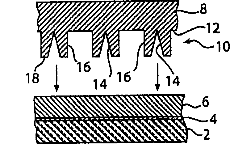
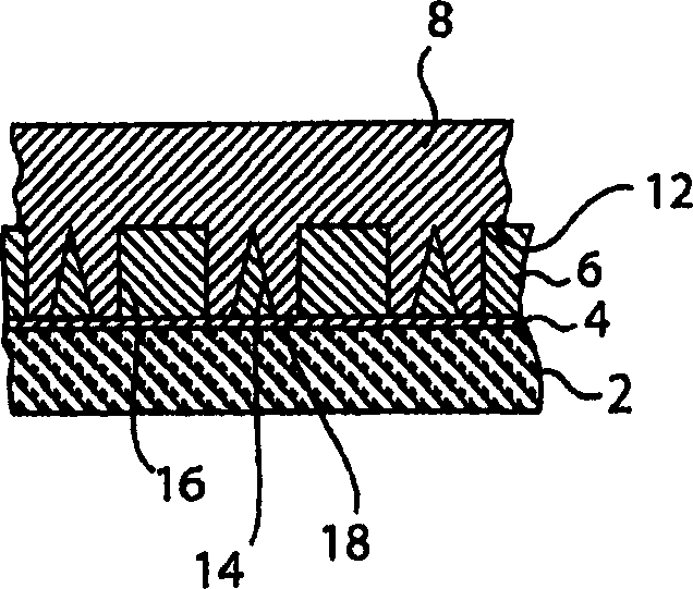
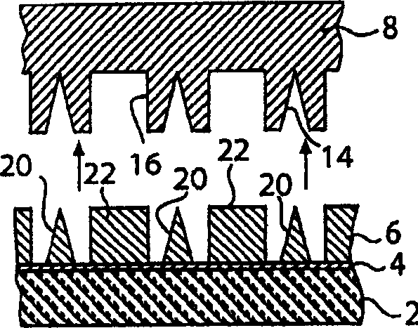
[0037] A gate structure (triode structure) for a field emission device is produced by means of an embodiment of the method according to the invention. In FIG. 1, the manufacture of a field emission device 1 having a triode structure is described.

[0038] A substrate 2 , for example a glass plate, firstly has an electrically conductive layer in the form of a patterned cathode 4 . The cathode 4 will form the first electrode in the triode structure. Such as Figure 1A As shown, a layer 6 of liquid material is disposed over the substrate 2 and the cathode 4 . Layer 6 preferably has a thickness between 1 and 10 micrometers and is deposited on substrate 2 by means of spin-coating processes, screen-printing techniques or dip-coating processes among others. The liquid material is preferably of the sol-gel type, such as suspensions of silica gel (Silica Sol TM50) and methyltrimethoxysilane (MTMS). Alternatively, the liquid material comprises polyimide with a photosensitive compoun...


PUM


Abstract

A field emission device ( 1 ) may be used for emitting electrons in, for example, a field emission display (FED). Field emission tips ( 40 ) are used for the emitting of electrons in the field emission device ( 1 ). In operation of the field emission device ( 1 ) a voltage is applied between a first electrode ( 4 ) having electrical contact with the field emission tip ( 40 ) and a second electrode ( 34 ) to make the field emission tip ( 40 ) emit electrons. To form a field emission tip ( 40 ) a layer of liquid material is applied on a substrate ( 2 ) provided with the first electrode ( 4 ). The layer of liquid material is embossed with a patterned stamp and subsequently cured to form a field emission tip structure ( 20 ). A conductive film ( 38 ) is applied on the field emission tip structure ( 20 ) to form a field emission tip ( 40 ) that has electrical contact with the first electrode ( 4 ).

Description

technical field [0001] The present invention relates to a method of manufacturing a field emission device. [0002] The invention also relates to a field emission device. Background technique [0003] Field emission devices can be used as electron sources for flat panel displays, so-called field emission displays (FED), which are vacuum electronic devices. [0004] Field emission is a quantum mechanical phenomenon in which electrons tunnel across a potential barrier at the outer surface of a suitable emissive material due to an applied electric field. The presence of an electric field confines the width of the barrier at the finite outer surface, with the result that the barrier is permeable to electrons. Therefore, electrons can be emitted from the field emission material. Field emission devices usually use a gate structure (also known as a triode structure). The gate structure consists of a field emission material and two electrodes, namely a cathode and a gate. In th...

Claims


Application Information

Patent Timeline
Patent Type & Authority Applications(China)
IPC IPC(8): H01J9/02H01J1/304H01J3/02
CPCH01J1/3044H01J3/022H01J9/025H01J2201/30407H01J2201/30426H01J2329/00H01J1/30
Inventor H·M·维斯塞M·A·维斯楚伦T·J·文克
Owner KONINK PHILIPS ELECTRONICS NV
Why Eureka
Try Eureka