


Quick Research
Generate reliable direction feasibility study reports for your R&D in just a few steps.

Technical Q&A
Discover and master advanced knowledge NOW. Basics, ideas, possibilities, all at once.

Find Solutions
As an expert in R&D theories, this can generate solutions to your technical problems instantly.

Evaluate Feasibility
Analyze your overall solution with one click, know your potential R&D risks in advance.

Monitor Landscape
Get weekly tech updates, stay abreast of the latest tech innovations and key insights.
Microraster structure
A micro-grating and grating technology, applied in the field of micro-grating structures, can solve problems such as poor actuation stability and poor synchronization
- Summary
- Abstract
- Description
- Claims
- Application Information
AI Technical Summary
Problems solved by technology
Method used
Image

Examples
Embodiment Construction
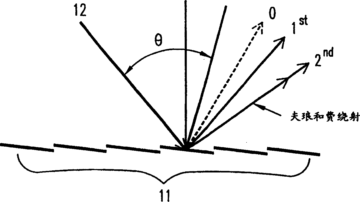
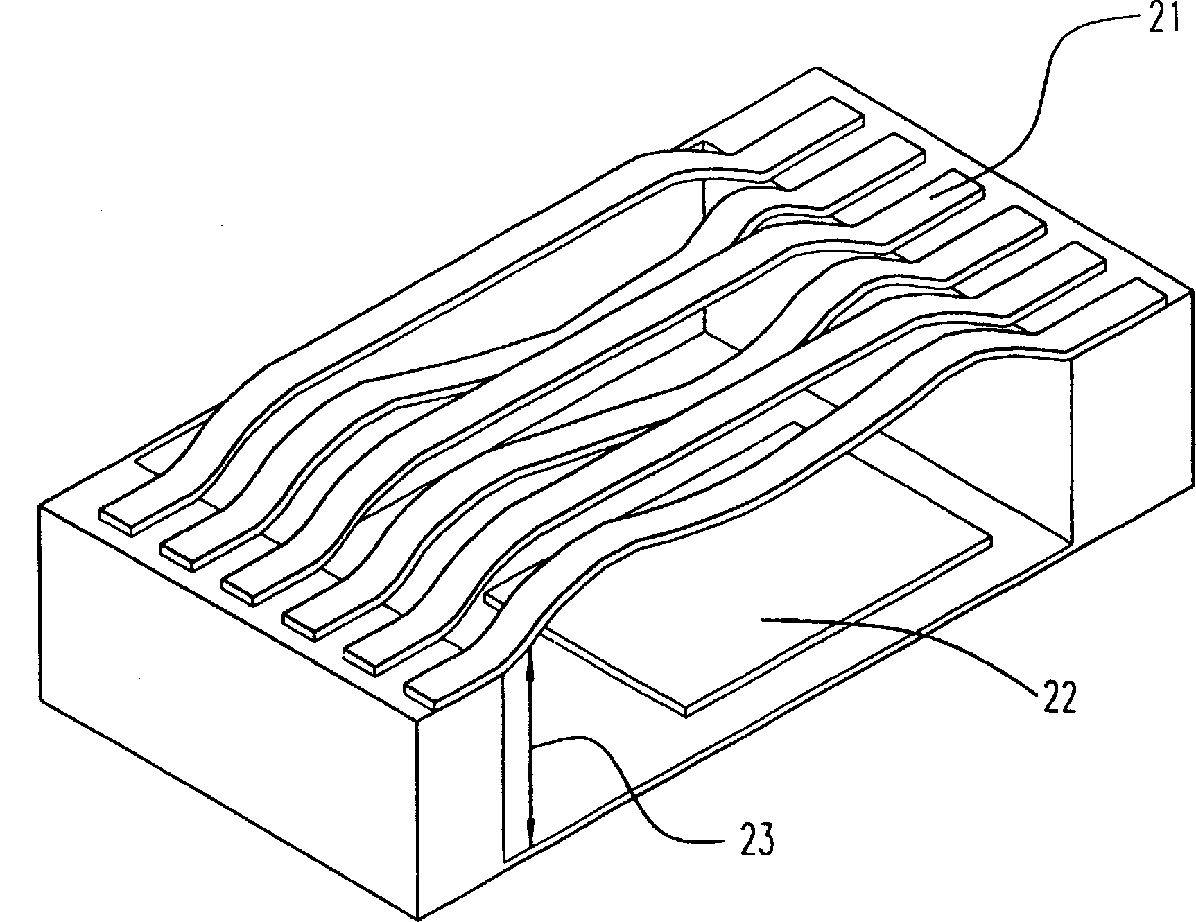
[0065] see Figure 6 , which is a top view of a preferred implementation of a micro-grating structure in the present invention. The micro-grating structure is composed of a semiconductor substrate 61, multiple pairs of structural pillars (wherein each pair of structural pillars is composed of a first structural pillar 62 and a second structural pillar 63), a plurality of gratings 64, a plurality of gaps 65, a first A support portion 66 and a second support portion 67 are formed, wherein the grating 64 also has a first torsion bar 641 , a second torsion bar 642 , a third torsion bar 643 and a fourth torsion bar 644 . The micro-grating structure is made of silicon as the material of the semiconductor substrate 61, and a plurality of gratings 64 are arranged between the first structural pillar 62 and the second structural pillar 63 of each pair of structural pillars, wherein each grating 64 is Adjacent to each other with a gap 65 less than 2 μm wide, and each grating 64 is conne...
PUM
 Abstract
Description
Claims
Application Information
 - R&D Engineer
- R&D Manager
- IP Professional
- Industry Leading Data Capabilities
- Powerful AI technology
- Patent DNA Extraction
Browse by: Latest US Patents, China's latest patents, Technical Efficacy Thesaurus, Application Domain, Technology Topic, Popular Technical Reports.
© 2024 PatSnap. All rights reserved.Legal|Privacy policy|Modern Slavery Act Transparency Statement|Sitemap|About US| Contact US: help@patsnap.com