Step-recursion nano-level measuring system based on high-precision inductive probe

An inductive probe, nano-scale technology, applied to the components of electrical measuring instruments, measuring electronics, measuring devices, etc., can solve the problems of complex structure of the measurement system, difficult adjustment, limited accuracy, etc., and achieve high measurement accuracy, Large measuring range, easy-to-achieve effects

Inactive Publication Date: 2006-05-31
INST OF AUTOMATION CHINESE ACAD OF SCI
View PDF0 Cites 0 Cited by
  • Summary
  • Abstract
  • Description
  • Claims
  • Application Information

AI Technical Summary

Problems solved by technology

Scanning probe microscopy techniques, such as scanning tunneling microscope (STM), atomic force microscope (AFM), photon scanning tunneling microscope (PSTM), etc., have certain requirements for the measurement object and can only give nanoscale resolution. However, the accurate nanometer size of the surface structure cannot be given; optical interference microscopy and F-D etalon-based micrometry technology have high measurement accuracy, but the measurement system has a complex structure, strict manufacturing requirements, and difficult adjustment; scanning X-ray interference The technology uses silicon as a linear scale, and is mainly implemented by combining X-ray interferometry and optical interferometry. Due to the uncertainty of X-ray wavelength, its accuracy is limited.

Method used


Image

  • Step-recursion nano-level measuring system based on high-precision inductive probe
  • Step-recursion nano-level measuring system based on high-precision inductive probe
  • Step-recursion nano-level measuring system based on high-precision inductive probe

Examples


Embodiment Construction

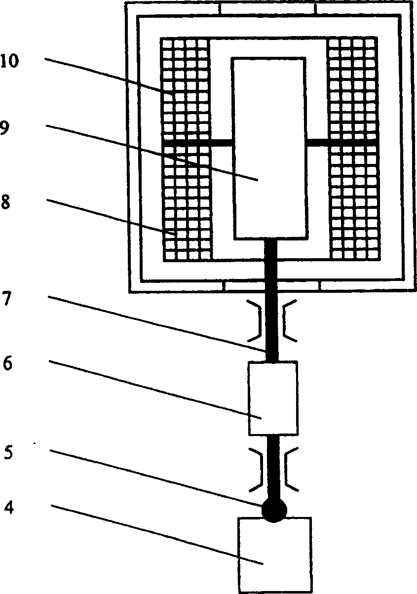
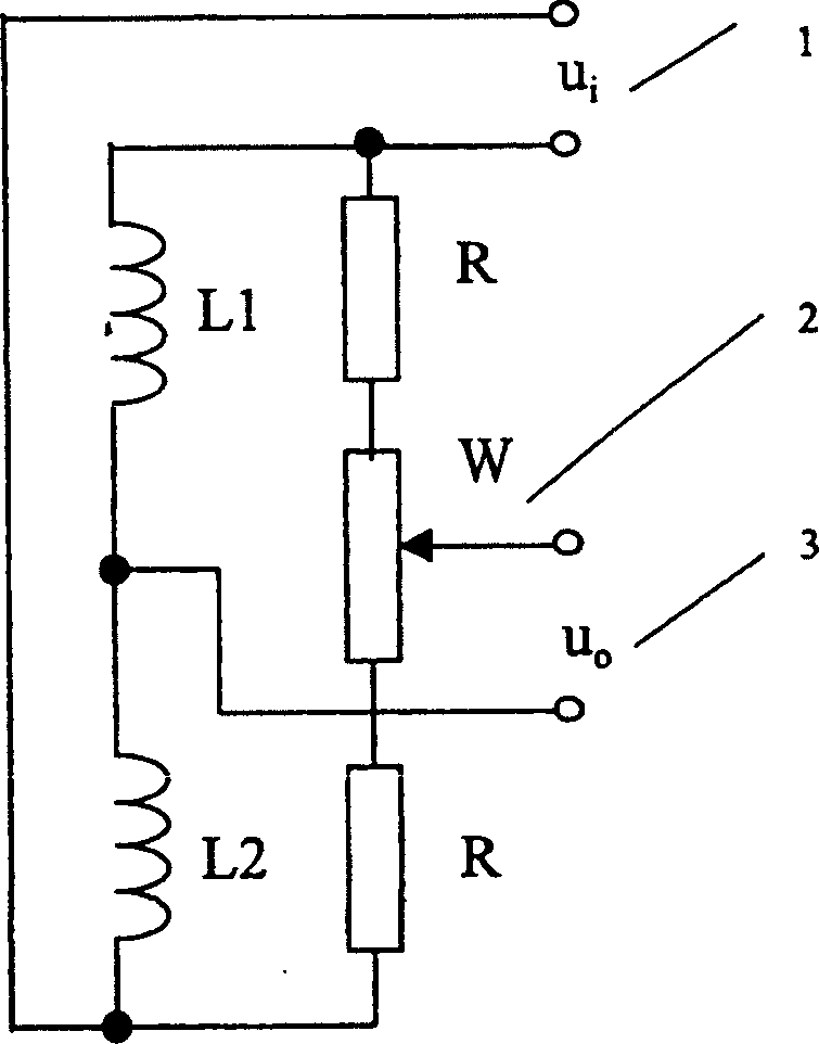
[0015] Such as figure 2 and image 3 As shown, the high-precision inductive probe adopts a differential method, and there are two coils 10 and 8 in the probe, that is, L1 and L2, and the iron core 9 is placed between the two coils. The iron core 9, the measuring rod 7, the micro-feeding device 6, and the measuring rod contact 5 are connected into one body, and it is ensured that the object 4 to be measured is in good contact with the inductive probe 5. If the slight change of the micro-feeding device 6 is not considered, when the displacement of the object 4 to be measured changes slightly, the iron core 9 will move up and down. Because the magnetic field distribution between the coils L1 and L2 is uniform, the iron core 9 moves Will cause the inductance of the two coils L1 and L2 to change by equal amounts but opposite signs. Under the excitation of the standard sine wave 1 with stable frequency and amplitude, the bridge circuit converts the inductance change into a voltag...


PUM


Abstract

A step-by-step recursive nanoscale measurement system based on a high-precision electric probe, including a control part, an iron core (9) placed between a first coil (10) and a second coil (8); a measuring rod (7 ), one end of which is connected to the iron core (9), and the other end is connected to the measuring rod contact (5); the upper and lower ends of the nano-scale micro-feeding device (6) are fixed on the measuring rod (7). The micro-displacement of the object (4) provides the feed amount; the control part controls the micro-feeding device (6) with nanometer-level precision according to the displacement of the object to be sided. The present invention adopts a step-by-step recursive method for micro-displacement measurement, on the one hand, the nano-level measurement is easy to realize, and on the other hand, the whole measurement system has a larger measurement range. Therefore, the nanoscale feeding device determines that the measurement system has high measurement accuracy. The measurement system adopts contact measurement, so this system is suitable for quasi-static micro-displacement measurement.

Description

technical field [0001] The invention relates to a nanometer-level measurement system, in particular to a step-by-step recursive nanometer-level measurement system based on a high-precision electric probe. Background technique [0002] Nano-measurement is a comprehensive interdisciplinary subject. Although there are many types of nano-measurement technologies developed in recent years, mature technologies are mainly classified into four categories: scanning probe microscopy, optical interference microscopy, scanning X-ray Interferometric technology, micrometric technology based on F-D etalon. Scanning probe microscopy techniques, such as scanning tunneling microscope (STM), atomic force microscope (AFM), photon scanning tunneling microscope (PSTM), etc., have certain requirements for the measurement object and can only give nanoscale resolution. However, the accurate nanometer size of the surface structure cannot be given; optical interference microscopy and F-D etalon-based...

Claims


Application Information

Patent Timeline
Patent Type & Authority Patents(China)
IPC IPC(8): G01B7/02G01D5/22G01R1/067
Inventor 台宪青胡旭晓杨克己
Owner INST OF AUTOMATION CHINESE ACAD OF SCI
Why Eureka
Try Eureka