
Storage device

A storage device and storage unit technology, which is applied in information storage, static memory, read-only memory, etc., to achieve the effect of shortening time and quickly putting into operation

Inactive Publication Date: 2005-09-07
INFINEON TECH AG
View PDF2 Cites 0 Cited by
  • Summary
  • Abstract
  • Description
  • Claims
  • Application Information

AI Technical Summary

Problems solved by technology

Conventional storage devices cannot yet meet this requirement

Method used


Image

  • Storage device
  • Storage device

Examples


Embodiment Construction

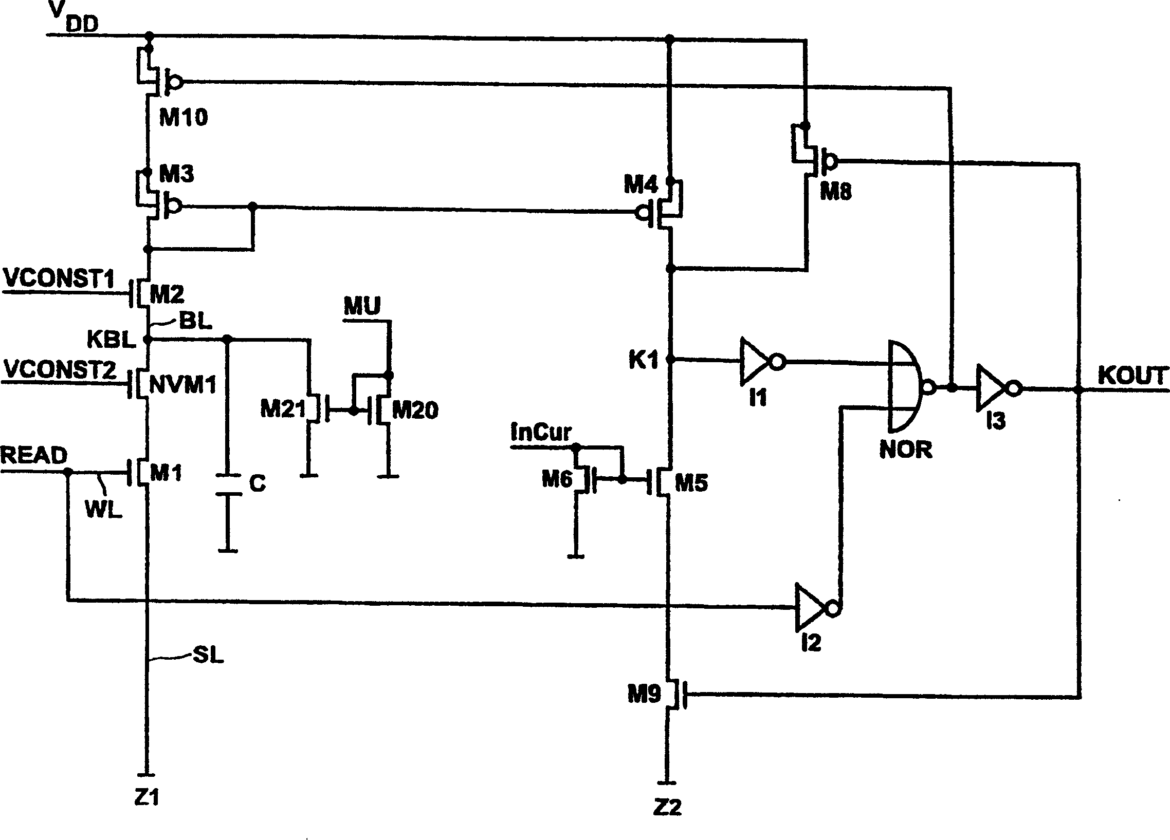
[0018] The memory devices discussed in detail below relate to an EEPORM. But it is not limited to this. The properties of the EEPROM described below can also be advantageously applied to any other non-volatile or volatile (semiconductor) memory devices, such as flash memory, RAM, etc.

[0019] The structure of the EEPROM discussed below is shown in the accompanying drawings.

[0020] For clarity, only one of the many memory cells that an EEPROM typically has is shown in the drawings.

[0021] The memory cell shown consists of a storage transistor designated with the reference symbol NVM1 and a selection transistor connected in series with it and designated with the reference symbol M1. The selection transistor M1 is connected to ground potential via the so-called source line SL, while the storage transistor NVM1 is connected to the supply potential V via the so-called bit line BL and transistors M2, M3, M10. DD connected.

[0022] The selection transistor M1 is controlled ...


PUM


Abstract

A description is given of a memory device having memory cells for storing data. The memory device described is distinguished by the fact that a current switch-off device is provided, which prevents an existing current flow through the memory cell to be read in response to the identification of the memory cell content, and / or that a discharge device is provided, which partly discharges again a node in the memory cell which is to be precharged before the memory cell is read.

Description

technical field [0001] The present invention relates to a memory device having memory cells for storing data and a read amplifier with the aid of the magnitude and / or direction of the current regulated by the memory cell when the memory cell is read The contents of the memory cell can be found. Background technique [0002] Many embodiments of this type of storage device have been known for many years. [0003] As in other relatively expensive circuits, when developing storage devices, efforts are also made to keep the energy consumption as low as possible or to reduce it further. Especially in recent years this aspect has achieved greater success. [0004] But for some applications, the energy consumption of storage devices has been very high. [0005] One such application is storage devices for contactless chip cards. [0006] As is known, contactless chip cards are exclusively wirelessly connected to other devices. The energy required for its operation is even transm...

Claims


Application Information

Patent Timeline
Patent Type & Authority Patents(China)
IPC IPC(8): G11C16/06G11C7/06G11C16/26
CPCG11C7/062G11C16/26
Inventor U·韦德H·-H·维赫曼恩
Owner INFINEON TECH AG
Learn More